Download this article as a .PDF
Packaging means different things to different people. For a device designer, it is an enclosure of almost microscopic size. For a systems-level engineer, it may be a series of racks that must fight on a battleship. No matter the size, electronic packaging is meant to provide mechanical protection while remaining electrically invisible.
When factors such as high production volumes come into play, then packaging goals must also be met with cost constraints. At the other extreme, electronic packaging for devices heading into outer space, such as on satellites, must endure temperature extremes and vacuum environments. Packaging is often taken for granted as part of an integrated-circuit (IC) design process, but the reliability and successful operation of that IC usually hinge on the quality of its package.
Higher-frequency packages must be considered as part of the circuits they enclose. For example, semiconductor die are typically either fully encapsulated in some form of epoxy-based compound, or else they are mounted in some form of cavity package formed of different materials (including metals, ceramic, and plastic).
In addition to an IC, the package may also contain passive impedance-matching components, bias circuitry, components for suppression of EMI, etc. The first method, of over-molding a device or IC in a polymeric material, is the most cost-effective packaging approach, but it requires significant tooling costs and is susceptible to high moisture absorption and high dielectric loss at RF/microwave frequencies.
Package complexity and materials contribute a great deal to its cost, and the RF/microwave industry has traditionally been faced with relatively mild demands in terms of volume for device packages compared to broader electronic industries, such as for power and computer applications. Packages for RF/microwave applications must also support wide bandwidths and high frequency ranges, and this has traditionally required costly package substrate materials, such as ceramic.
Higher-volume device packaging has turned to enclosing conductive metal leadframes with lower-cost plastic materials, and many of these plastic packages are finding application for RF/microwave devices. One challenge facing all high-frequency device package developers is the production of lower-cost package solutions capable of working well into the millimeter-wave frequency range, but also with the durability to survive long-term use in hostile operating environments, such as in automotive electronic safety systems.
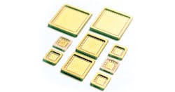
Within lower microwave frequency ranges, one of the more popular device packages at present is the quad, flat, no-leads (QFN) package (Fig. 1). It is small in size and relatively low in cost. A QFN package allows for attachment and connection of an IC to a PCB without through-hole connections, using surface-mount technology (SMT) for compatibility with PCBs using microstrip and coplanar-waveguide (CPW) transmission-line technologies.
Such a package consists of a leadframe, wire bonds, and a molding compound as a cover. The lead frame is formed of a conductive copper alloy for low-loss electrical connections. A thermally conductive adhesive attaches the device to be packaged to the leadframe thermal bead. Gold bond wires are used for electrical connections from the device’s leads to the package leadframe.
QFN packages are available in two formats: plastic molded QFNs and air-cavity QFNs. A plastic-molded QFN is basically a copper leadframe with a plastic cover and is typically usable to about 3 GHz. An air-cavity QFN package, which consists of a copper leadframe, plastic molded body (open and not sealed), and either a ceramic or a plastic lid, is usable to about 20 GHz.
Air-cavity packages have been developed in many configurations, including for optical and photonic devices—as well as for relatively new device technologies such as microelectromechanical-systems (MEMS) devices, in which mechanical and electrical functions must be supported.
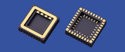
These packages are usually based upon ceramic materials and may be a simple as “can-like” structures to hold a device, such as leadless chip carriers (LCCs). More often, custom packaging is required for MEMS devices, which has encouraged the use of package designs with premolded thermoplastic leadframes that preserve both cost and performance while providing the flexibility of rapid design modifications to meet the needs of a multiple-contact MEMS device (Fig. 2). One of the thermoplastic materials used in high-frequency device packages is liquid crystal polymer (LCP), which is favored for its low moisture absorption and low dissipation factor (low loss).
Manufacturing process temperatures will play a part in the selection of package materials, such as the elevated temperatures required for lead-free (RoHS-compliant) soldering processes. Ceramic materials such as alumina, for example, have very high firing temperatures (about +1,600ºC) which will limit the choice of metallization (to tungsten) for package leads since most metals can’t survive such a high firing temperature.
By blending ceramic materials with other materials, such as glass as used in low-temperature-cofired-ceramic (LTCC) packages, the firing temperature of the ceramic composite can be reduced to about +700 to +800ºC, in contrast to the much higher firing temperatures of high-temperature-cofired-ceramic (HTCC).
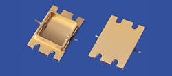
As the power of the packaged circuit or device increases, the thermal capacity of the package must follow. In higher-power RF/microwave device packages, thermal design is given as much attention as electrical design. Device packaging for RF/microwave discrete power transistors must provide low-loss electrical connections that are stable at high power levels. This usually means also dissipating large amounts of heat. High-power transistor packages are usually identified by large mounting areas to a PCB, such as flange-mount attachments, to allow maximum flow of heat away from the transistor or other active device (Fig. 3).
MM-Wave Packages
Package developers are often challenged by emerging technologies and trends. With so much attention being paid to the next, Fifth Generation (5G) of wireless communications, and its uses of new and different frequency bands than past generations of wireless systems, there is concern about how to cost-effectively package active devices operating at millimeter-wave frequencies for use in those 5G systems.
One company that has been instrumental in driving performance levels for millimeter-wave packages is StratEdge (www.stratedge.com). The firm has been a pioneer in addressing the high-power-density requirements of RF/microwave GaN devices, using high-power laminate copper-moly-copper (CMC) base packages to promote consistent heat flow away from GaN devices, whether as discrete or monolithic-microwave-integrated-circuit (MMIC) devices. The packages are also suitable for other high-frequency semiconductor processes, such as gallium arsenide (GaAs) and silicon carbide (SiC) capable of producing high-frequency devices with high-power output levels.
At the recent 2017 IMS, StratEdge announced additions to its LL family of high-frequency packages, which combine the thermal requirements of high-power packaging with the extended-frequency performance needed for millimeter-wave devices (Fig. 4). The packages support discrete and MMIC device applications from DC to 63 GHz in applications requiring high-power millimeter-wave signals, including commercial and military radar systems.
The LL packages are available in leaded and leadless versions. They are either flangeless, with a hermetic seal and ceramic lid, or with flanges for mounting on a PCB for effective thermal transfer. The company also offers complete automated assembly and test services for the high-power, high-frequency packages.


