UWB Printed Antenna Blocks Satellite and WLAN Signals
This file type includes high resolution graphics and schematics when applicable.
Ultrawideband (UWB) communications systems provide many times the bandwidth needed for standard communications services, such as cellular wireless communications or wireless local area networks (WLANs). One of the main benefits of an UWB component like an antenna or amplifier is that a single component can be used in a system that provides multiple communications services.
As an example, a novel printed UWB monopole antenna was developed with dual-notched frequency bands, for use in both the 5.2-GHz WLAN band and the 8.0-GHz X-band satellite-communications (satcom) band. The design couples an E-shaped structure with microstrip feedline to achieve UWB performance with band-rejection capability. The UWB antenna demonstrates omnidirectional radiation patterns across its wide bandwidth.
UWB radio technology has attracted a great deal of attention ever since the U.S. Federal Communications Commission (FCC) allocated 7.5 GHz of bandwidth (3.1 to 10.6 GHz) for unlicensed radio applications. Many applications have been developed based on UWB technology, such as short-range broadband communications, radar sensing, and body-area networks (BANs) for medical and health-care use.1 In terms of antennas for UWB systems, planar monopole antennas present attractive features: simple structure, small size, low cost, stable radiation patterns, and constant gain over wide operating bands. Owing to these characteristics, research is increasingly being focused on planar monopoles for UWB use.2-6
Potential problems for UWB communications systems stem from interference from existing systems within that wide frequency range, such as 5.8-GHz signals from WLAN systems and 8-GHz signals from X-band satellite communications systems (XSCSs). As a result, a compact UWB monopole antenna with multiple reject bands can provide a practical solution to reject these unwanted interference signals.7-13
To achieve the desired band-notched performance, different-shaped slots (such as U- or V-) are usually inserted into the initial UWB monopole antenna structure. In refs. 8 and 9, however, only one notch band was created. In refs. 10 and 11, two notched bands can be achieved by means of a defected ground structure (DGS) approach. However, all these notched UWB antenna design strategies are based on the use of multilayer circuit structures that would increase fabrication costs and not be compatible with existing integrated-circuit (IC) radio devices.
To provide a practical solution for limiting the effects of interference in UWB systems, a compact UWB monopole antenna with two notch bands was developed. To start, the resonant properties of an E-shaped resonator were explored. Analysis of the resonator structure reveals that dual bandstop performance was possible based on the dual-mode resonant properties of the E-shaped resonator. By placing the E-shaped resonator structure close to the feedline of the UWB antenna, it should be possible to achieve the two notched bands within the total UWB frequency range.
To validate the design concept, a novel planar UWB antenna with two sharply rejected notch bands centered at 5.8 and 8.0 GHz, respectively, was designed and fabricated. Computer simulations and prototype measurements show that the antenna achieves an ultrawide bandwidth ranging from 2.0 to 11.0 GHz while avoiding interference from WLAN/XSCS signals. The antenna offers an omnidirectional radiation pattern in the H-plane across its full bandwidth.
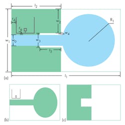
Figure 1 presents the geometry of the proposed UWB antenna with two sharp notch bands. The antenna consists of a dual bandstop filter and a conventional planar circular monopole antenna. It is fabricated on 0.508-mm-thick RO4350B circuit material from Rogers Corp. The circuit material exhibits a dielectric constant (relative permittivity) of 3.48 at 10 GHz in the z-axis (thickness) of the substrate. The bandstop filter (i.e., the two notch bands) is realized by coupling the E-shaped resonator to 50-Ω microstrip feedlines for the antenna.
The proposed planar UWB antenna has a circular patch with radius, R1 , of 8.5 mm, which is fed by 50-Ω microstrip line of width w0 = 3.5 mm. To improve impedance-matching performance, a rectangular slit is embedded in the ground plane, located under the microstrip feed line. The final optimized parameters of the planar UWB antenna are as follows: w1=20 mm, w2=8.05 mm, w3=4.6 mm, w4=0.3 mm, l1=35 mm, l2=16 mm, and l3=3.8 mm.
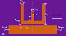
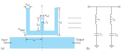
The proposed E-shaped resonator is composed of a stepped-impedance hairpin resonator with a centrally loaded short-ended stub. Figure 2 shows the layout of the E-shaped resonator coupled to a section of main transmission line and its corresponding equivalent circuit. The properties of the E-shaped resonator can be analyzed by the even-odd-mode analysis method. Under mode excitation, the electrical field distribution of the resonator exhibits either an even- or an odd-mode distribution property. Thus, the even- and odd-mode resonant frequencies (feven and fodd, respectively) can be deduced by means of Eqs. 1 and 2, respectively:
where f is the center frequency of the E-shaped resonator; εeff denotes the effective dielectric constant of the substrate; and c is the speed of light in free space.
The dual-mode stepped-impedance resonator (SIR) can achieve dual-stopband (i.e., the two notch bands) performance when placed next to the microstrip feedline. It can be functionally equivalent to two shunt-connected series resonance circuits, as shown in Fig. 2(b). The section le1, le2 of the dual-mode SIR can be seen as the capacitance C while the section le3 of the dual-mode SIR can be seen as inductance L. The dimensions of the E-shaped resonator were selected as follows: we1 = 0.2 mm, we2 = 0.2 mm, le1 = 3 mm, le2 = 4.6 mm, le3 = 0.8 mm, and re = 0.2 mm.
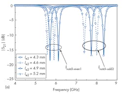
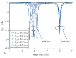
Transfer characteristics of the coupled E-shaped resonator with various dimensions were studied to validate its two-mode resonant properties (Fig. 3). The frequencies of the two notch bands move down simultaneously with increases in the length le1. This is because the electrical fields are distributed on these two sections for both the even and odd modes.
When le3 is decreased, only the frequency of the first notch band moves higher. This is because there are no electrical fields distributed on the area of le3 for the odd mode. Therefore, by appropriately adjusting the resonator dimensions, two notch bands can be achieved at desired frequencies.
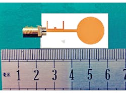
Based on the two bandstop filters previously described, a novel planar UWB monopole antenna with two high-rejection notch bands was designed as shown in Fig. 4. All simulations were carried out using Version 11.0 of the commercial Ansoft HFSS finite-element EM simulation software from Ansys.
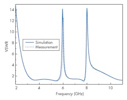
Figure 5 compares the simulated and measured VSWR for the UWB antenna. The antenna exhibits an impedance bandwidth of 2.0 to 11.0 GHz for a VSWR of less than 2.0:1, except for the notch bands of 5.5 to 6.5 GHz and 7.6 to 9.1 GHz. The center frequencies of these two notch bands are about 5.8 and 8.0 GHz, respectively.
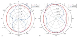
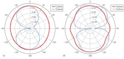
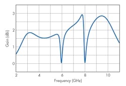
These notch bands are well suited for rejecting 5.8-GHz WLAN signals and 8.0-GHz satellite signals. The normalized radiation patterns in the E- and H-planes were simulated at 2.5, 5.0, 7.5, and 10.0 GHz (Fig. 6). As the patterns show, the antenna achieves good omnidirectional radiation patterns in the H-plane. Figure 7 plots the measured peak gain in the E-plane. The radiation patterns in the E-plane are in symmetry. Even with its dual notches, this antenna behaves very much like a typical printed-circuit-board (PCB) monopole antenna.
By controlling the parameters of the E-shaped resonator, the two notch bands can be easily tuned to the desirable frequency locations. The antenna covers the frequency range for UWB systems, between 2.0 and 11.0 GHz, with rejection bands centered around WLAN/SCS services. With the benefit of small size, outstanding performance can be realized for broadband antennas—widely needed for UWB applications.
The measured results show good performance in terms of reflection coefficient, antenna gain, and radiation patterns. The antenna design represents a practical approach for modern UWB wireless communication systems owing to its simple topology, compact size, and excellent performance.
Editor’s Note: The authors’ design approach was also demonstrated in the construction of an UWB bandpass filter, using parallel U-shaped slots to achieve dual frequency notches within the full FCC-approved UWB frequency range of 3.1 to 10.6 GHz.
Junding Zhao, Microwave Engineer
Hao Zhang, Microwave Engineer
Nanjing Changfeng Aerospace Electronic Technology Co. Ltd., Nanjing 210094, China
References
1. Revision of Part 15 of the Commission’s Rules Regarding Ultra-Wideband Transmission Systems, First Note and Order, Federal Communications Commission, ET-Docket 98–153, 2002.
2. M. Naghshvarian-Jahromi, “Novel wideband planar fractal monopole antenna,” IEEE Transactions on Antennas & Propagation, Vol. 56, No. 12, 2008, pp. 3844-3849.
3. M. Naser-Moghadasi, H. Rousta, and B.S. Virdee, “Compact UWB planar monopole antenna,” IEEE Antennas and Wireless Propagation Letters, Vol. 8, 2009, pp. 1382-1385.
4. S.M. Mazinani and H.R. Hassani, “A novel broadband plate-loaded planar monopole antenna,” IEEE Antennas and Wireless Propagation Letters, Vol. 8, 2009, pp. 1123-1126.
5. M. Sun, Y.P. Zhang, and Y. Lu, “Miniaturization of planar monopole antenna for ultrawideband radios,” IEEE Transactions on Antennas & Propagation, Vol. 58, No. 7, 2010, pp. 2420-242, 2010.
6. Raj Kumar, and Ashish G. Kokate, “On the design of square shape fractal antenna with matching strip for UWB applications,” International Journal of Electronics, Vol. 100, No. 7, 2013, pp. 881-889.
7. W.-S. Lee, D.-Z. Kim, K.-J. Kim, and J.-W. Yu, “Wideband planar monopole antennas with two band-notch characteristics,” IEEE Transactions on Microwave Theory & Techniques, Vol. 54, 2006, pp. 2800-2806.
8. K. Chung, J. Kim, and J. Choi, “Wideband microstrip-fed monopole antenna having frequency band-notch function,” IEEE Microwave & Wireless Component Letters, Vol. 15, 2005, pp. 766-768.
9. Y. Kim and D.H. Kwon, “CPW-fed planar ultra wideband antenna having a frequency band notch functions,” Electronic Letters, Vol. 40, 2004, pp. 403-405.
10. K. Yin and J. P. Xu, “Compact ultra-wideband antenna with two bandstop characteristic,” Electronic Letters, Vol. 44, 2008, pp. 453-454.
11. Dan-Hong Bi, Zhi-Yuan Yu, Shao-Guo Mo, and Xun-Cai Yin, “Two new ultra-wideband antennas with 3.4/5.5-GHz two band-notch characteristics,” Microwave & Optical Technology Letters, Vol. 51, 2009, pp. 2942-2945.
This file type includes high resolution graphics and schematics when applicable.
