GaN Devices Raising the Output-Power Performance Bar
Download this article in PDF format.
What you'll learn:
- What are the different materials are used in creating GaN power transistors?
- The impact of heat on performance.
- A rundown of high-power RF GaN transistors currently on the market.
Solid-state power comes in many forms, although the fastest-growing high-frequency, high-power semiconductor technology may be based on gallium nitride (GaN). GaN power transistors have long been the active-device building blocks for linear and compressed power amplifiers in L- and S-band military radar systems.
Depending on design needs, GaN power transistors are available from many suppliers for a variety of applications in circuits and systems for avionics, commercial, industrial, medical, and military use. They all leverage the capabilities of wide-bandgap GaN semiconductor materials to form RF/microwave transistors with high power density and high output-power levels in small packages.
Some GaN power transistors are available as bare die while many are supplied within rugged packages that have internal impedance matching to optimize output power for a particular frequency range. The frequency coverage for GaN transistors is approaching millimeter-wave (mmWave) frequencies at lower output-power levels; the highest output-power levels are still for pulsed signals typically at L- and S-band frequencies.
Materials Matter
Discrete GaN power transistors vary in form and function, even in the materials supporting the GaN semiconductor material foundation. Wide-bandgap GaN materials support different transistor structures, such as field-effect-transistor (FET), heterojunction-bipolar-transistor (HBT), and high-electron-mobility-transistor (HEMT) structures.
However, because of the high thermal resistance and limited power-dissipation capabilities of GaN material, GaN semiconductors are fabricated on substrates with lower thermal resistance, including GaN on silicon (Si), silicon carbide (SiC), and even synthetic diamond. The use of diamond materials, with the lowest thermal resistance of the three substrates, is motivated by research funding from DARPA and its Near Junction Thermal Transport (NJTT) program that’s been in place with several partners for over a decade.
Although it has extremely low thermal resistance, which aids in removing heat from the junction regions of GaN semiconductors, synthetic diamond still isn’t a practical substrate option for consumer/commercial applications of GaN devices or even for military/aerospace apps. The thermal properties of the three substrate materials are much different, with Si providing the least heat dissipation at the lowest cost and synthetic diamond the best thermal dissipation at the highest cost. Representing a practical tradeoff between cost and thermal performance, SiC is an often-used substrate for higher-power discrete GaN transistors, especially those intended for mission-critical applications.
As mentioned, discrete GaN power transistors are available as semiconductor die and in various package styles, some with input and input/output impedance matching to 50 Ω to simplify addition to RF/microwave circuits. GaN devices are becoming more common at lower frequencies as the active devices in high-voltage power supplies and power converters and in battery-charging applications.
Discrete devices in die form can handle wideband that nearly spans from dc to 18 GHz, while both die and packaged parts are available from near dc to mmWave frequencies, albeit at lower output-power levels at rising frequencies. GaN has become a well-accepted power-amplification technology in many pulsed radar applications, notably for power amplifiers (PAs) at C-, L-, and S-band frequencies. The technology is capable of high gain with little droop in pulse amplitude across frequency. It also provides extremely high drain efficiency or power-added efficiency (PAE) whether in chip or packaged form.
Just how much RF/microwave output power can be expected from a single GaN transistor? Practical PAs for radar and telecommunications amplifiers typically combine multiple active devices in driver and output stages to achieve a required peak/pulsed or continuous-wave (CW) output power for a design frequency and bandwidth. A single transistor will not be enough for a radar amplifier. But as higher-power discrete transistors become available, less active devices will be needed for the targeted output power.
Issues with Heat
Heat is usually a limiting factor in the power provided by a single transistor. Because the semiconductor junctions of a GaN transistor generate heat, especially at higher power levels, the heat must be managed to ensure a long transistor operating lifetime.
The amount of heat generated by a GaN (or any other) transistor will be determined by how efficiently it uses its power supply. Transistor drain efficiency refers to the amount or percentage of dc power supplied at the input (drain) of a transistor that’s available as RF signal power at its output. Amplifier designers and other users of transistors may refer to PAE, which considers the gain of the transistor and how well the amplifier’s circuitry uses the applied power.
If 100% efficiency were possible, a transistor could increase the power level of an input signal as a function of the device gain without dissipating any heat. But the drain efficiency is never 100% and some input power and bias energy will be lost as heat. The highest efficiency results in the least amount of heat that must be dissipated for safe and prolonged operation of the device.
Although some commercial GaN transistors feature good drain efficiency of 65% and higher, applied energy is lost as heat; thus, the heat must be dissipated for optimum transistor lifetime and performance. Packages with low thermal resistance can help to flow heat away from a transistor’s junctions.
The amount of output power available from a single GaN transistor will depend on the supply voltage (typically +28, +40, or +50 V dc), the size and shape of the package, and, for unpackaged die, how well they are thermally managed on an application circuit. Some GaN transistor suppliers offer semiconductors from the same process (such as for a +28-V dc supply) in two different packages, typically rugged metal-ceramic flange-mount packages and smaller “bolt-down” metal-ceramic packages. The basic tradeoff is power for size, with the transistor in the larger package able to deliver more output power by surrounding the transistor’s thermal junctions with a greater amount of heat-dissipating material.
Seeking a Source
Suppliers of high-power discrete RF GaN transistors that can power pulsed radar systems include BeRex, Cree, Integra Technologies, Microsemi, NXP, and Qorvo. Most of these discrete devices are designed for use at one of three supply (device drain-to-source) voltages: +28, +40, and +50 V dc.
BeRex, for example, offers three GaN-on-SiC power HEMTs in its BCGxxx series in die form for use with +28-V dc supplies. These are broadband devices with total frequency coverage of dc to 26 GHz that can be impedance-matched within amplifier circuits for applications at C-, X-, Ku-, and K-band frequencies. The three transistors, models BCG002, BCG004, and BCG008, provide saturated output-power levels of 2, 4, and 8 W, respectively, at a test frequency of 12 GHz, with better than 8-dB gain and PAE of 72%.
Most GaN discrete transistor suppliers provide their devices within power packages that are impedance-matched for high gain across a specific frequency range. For convenience, some even house the same GaN semiconductor within multiple package formats. For example, a high-power GaN-on-SiC HEMT from Integra Technologies that delivers 500-W peak output power at 2.856 GHz is available in a bolt-down package (model IGN2856S500) and in a heavy-duty flange-mount package (model IGN2856S500S).
Both packaged transistor versions are hermetically sealed with ceramic-epoxy lids and operate on supply voltage of +50 V dc. While the metal flanges add size compared to the bolt-down package, the amount of ceramic material in both packages is the same, arming them with similar thermal-dissipation characteristics.
Each packaged device contains impedance-matching circuits at input and output ports for optimum performance at the 2.856-GHz industrial, scientific, and medical (ISM) frequency, achieving 60% typical drain efficiency with 12-μs-wide pulses at 3% duty factor. The power transistors handle input-signal power levels from 25.0 to 39.7 W and provide typical gain of 11.8 dB.
Available for several years for C-band pulsed radar amplifiers, the 3942GN-120V GaN-on-SiC HEMT from Microsemi provides 120-W peak output power from 3.9 to 4.2 GHz when powered by a +50-V dc supply. The reliable gold-metallized transistor is housed within a hermetically sealed flange-mount package. When characterized with 200-μs-long pulses at 10% duty cycle, it operates with typical drain efficiency of 62%. The gain is high, typically 15.2 dB at 3.9 and 4.2 GHz, with little pulse droop, typically −0.15 dB or better.
For those requiring wider bandwidth, albeit with much less power, the same company’s model DC35GN-15-Q4 is a GaN-on-SiC HEMT designed in a Class AB linear configuration for use in both pulsed and CW applications from 5 MHz to 3.5 GHz. Across that frequency range, it provides typical output power of 19 W with CW signals or with pulses as wide as 1000 μs at 10% duty cycle. Supplied in a compact air-cavity QFN package, the discrete transistor supports radar and communications systems applications with typical drain efficiency of 66%. It’s designed for +50-V dc supply voltage.
Another wideband high-power GaN-on-SiC discrete transistor, the MMRF5017HS from NXP Semiconductors, is supplied in a bolt-down metal-ceramic package with input impedance matching for use from 30 to 2200 MHz. The versatile +50-V dc power transistor can handle CW and pulsed signals with high efficiency and gain. It delivers 125-W CW output power and 18-dB typical gain with 59.1% drain efficiency at 520 MHz and 80-W CW output power, 18.4-dB gain, and 44% drain efficiency at 940 MHz. When tested with 2200-MHz, 100-μs pulses for a 20% duty cycle, it provides peak output power of 200 W.
Offering slightly more power over a wider bandwidth and in a more conventional flange-mount package, the same company’s model MMRF5014H is a discrete GaN transistor capable of CW and pulsed operation from 1 to 2700 MHz. It features peak and CW output power of 125 W at 2500 MHz with 16-dB CW gain and 18-dB pulsed gain. The drain efficiency is 64% or better for both CW and pulsed (100-μs pulses at 20% duty cycle) signals. When tested for wideband operation, it’s capable of 100-W CW output power with 12-dB gain from 200 to 2500 MHz, although the typical drain efficiency drops to 40%.
The QPD1029L discrete GaN-on-SiC power transistor developed by Qorvo is among the highest-voltage GaN RF power transistors, designed for supply voltage of +65 V dc. Its input matches a pair of GaN die within a four-lead flange package for high signal power levels from 1.2 to 1.4 GHz. Ideal for L-band pulsed-radar applications but also useful for boosting CW signals, the device achieves 1500-W output power with 300-μs-wide pulses at 10% duty cycle. The output power is a result of 21.3-dB linear gain for an input signal at +46.2 dBm. Typical drain efficiency at 1.3 GHz is 62.5%.
Many of these discrete GaN transistors employ gold metallization for high reliability and are rated for maximum drain-source (supply) voltage of +150 V dc. As the examples show, significant peak output power is possible from a single device operating on any one of the three most popular supply voltages (+28, +40, and +50 V dc)—operation at a higher supply voltage is no guarantee of higher output power.
In fact, reliability studies using accelerated life testing (by Cree)1 revealed that GaN-on-SiC HEMTs handled different supply voltages equally well. Even at the highest supply voltage (+50 V dc), while some devices exhibited slight degradation in saturated output power, possibly due to burn-in behavior, no failures were found during accelerated life testing of transistors fabricated with several different GaN-on-SiC processes.
Cree offers the widest assortment of GaN-on-SiC discrete transistors, in both die and packaged versions. In die form, the CGHV1J025D discrete GaN-on-SiC transistor provides enough (saturated) output power at 25 W from 10 MHz to 18 GHz to serve a variety of point-to-point and satellite communications and marine radar applications. When tested at +40 V dc in a test fixture, the transistor yields 17-dB small-signal gain and 60% typical PAE at 10 GHz. For more power and the same amount of gain but less bandwidth, the firm’s CGHV60040D GaN power transistor die delivers 40-W output power with 65% PAE from dc to 6 GHz and a +40-V dc supply.
Pick a Package
Addressing layout flexibility, Cree houses many of its discrete GaN-on-SiC transistors in flanged and flange-less pill packages. For example, the +50-V dc model CGHV40100 comes in both package styles with equal performance levels from dc to 3 GHz for each of the packaged devices.
The discrete power transistors, available from distributor Mouser Electronics, require input- and output-impedance matching for a particular application. They’re capable of 100-W saturated CW output power at 1 GHz, 141 W at 1.5 GHz, and 116 W at 2.0 GHz, with 16.9-dB small-signal gain at 1 GHz and 17.5-dB gain at 2 GHz. The transistor provides the high efficiency that GaN is known for, with drain efficiency of 68% at 0.5 GHz, 56% at 1 GHz, and 54% at 2 GHz.
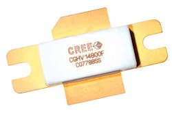
Among its packaged devices, Cree’s CGHV14800 GaN HEMT (Fig. 1) is one of the highest-power discrete devices available, targeting pulsed L-band air-traffic control and weather radars from 960 to 1400 MHz. Supplied in a rugged ceramic/metal flange package, it delivers 1000-W output power with 15.5-dB typical gain and 74% typical drain efficiency at 1.2 GHz.
At its upper-frequency limit, the +50-V dc transistor still provides 910 W output power and 15.1 dB gain with 67% typical drain efficiency at 1.4 GHz. It handles pulsed input-power levels at +41 dBm for 100-μs pulses at 5% maximum duty cycle and suffers only −0.3-dB pulse amplitude droop across its bandwidth.
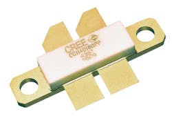
For a lower-voltage supply, the model CGH40180PP from Cree is an unmatched GaN-on-SiC HEMT in a four-lead flange package (Fig. 2) designed for use from dc to 3 GHz with +28 V dc drain voltage. An effective signal power booster for cellular infrastructure and test system applications, it delivers 220-W typical saturated CW output power from 1.1 to 1.3 GHz with 65% typical drain efficiency and 13-dB minimum power gain. The small-signal gain is typically 20 dB at 1 GHz and 15 dB at 2 GHz.
Of course, these represent just a few examples of the high-power RF/microwave capabilities of GaN and GaN-on-SiC substrates. GaN on Si is a foundation for a growing number of power-conversion and charging products keyed by companies such as Texas Instruments and GaN Systems. Texas Instruments’ +600-V dc GaN FETs with integrated drivers have become key components in many power-supply and power-conversion products. GaN Systems offers a +650-V dc GaN HEMT die for high-power-density power converters and motor drives.
GaN provides high signal power at RF and microwave frequencies and is likely to move steadily into the mmWave frequency range as signal power needs grow for applications such as 5G wireless cellular communications and automotive radar systems.
Reference
1. Donald A. Gajewski, Scott Sheppard, Simon Wood, Jeff B. Barner, Jim Milligan, and John Palmour, “Reliability Comparison of 28 V – 50 V GaN-on-SiC S-Band and X-Band Technologies,” Wolfspeed, a Cree Company.


