High-Voltage GaN-on-Si Devices Deliver High Power
This file type includes high resolution graphics and schematics when applicable.
Gallium-nitride (GaN) semiconductor devices offer great promise for designers of high-frequency active circuits, especially when high output-power levels are needed at higher frequencies. GaN devices offer the mobility and transconductance of gallium arsenide (GaAs) active devices, with the added capability of operating at high voltage levels to achieve high output-power levels. As with silicon laterally diffused metal-oxide-semiconductor (LDMOS) devices, GaN active devices are capable of output-power levels of tens to hundreds of watts, but with a fraction of the input and output capacitances of those Si LDMOS devices, for high output power over broad bandwidths and with high efficiency.
With +48-VDC GaN devices now available, design engineers have further options using for GaN devices in commercial and military applications. Understanding the differences between these emerging +48-VDC GaN devices compared to existing +28-VDC GaN devices can help in matching these higher-voltage devices to suitable applications.
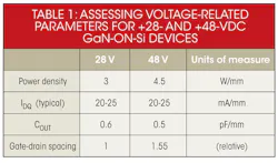
These higher +48-VDC drain supply voltages offer both obvious and subtle benefits. Because device channel size is largely set by peak current requirements, a higher supply voltage reduces the transistor size required for a given RF power rating. Table 1 shows how power density, as measured by gate periphery for typical GaN-on-Si devices, approximately scales by the voltage ratio.
Migrating existing +28-VDC processes to allow for +48-VDC operation requires redesigning the device structure to improve reliability due to the increased electric field. In the X-Y direction, the underlying substrate, epitaxial structure, and channel characteristics remain largely the same for higher-voltage operation, with increased gate-to-drain spacing needed to raise the breakdown voltage. In the Z-direction (vertically), the gate oxide is thickened and changes to the gate metal allow for both higher reliability and increased standoff voltages.
Of greater importance to RF/microwave amplifier designers, Table 1 shows that device output capacitance (COUT) scales by device size. Because of the increased power density, the resulting COUT) for a given power level is reduced. This reduction in output capacitance is the largest differentiator for higher-voltage operation since the resulting change in load impedance offers a major advantage in device operation.
Perhaps the biggest challenge that designers face at higher power levels and frequencies is matching the low output impedances of larger devices. A parallel resistor-capacitor (R-C) circuit is a good model for the transistor output, corresponding to the equivalent R with COUT as specified in Table 1. Given the supply voltage (V) and desired power (P) of an ideal amplifier, there is a simple equation that estimates the output resistance (ROUT):
P ≈ V2/2ROUT (1)
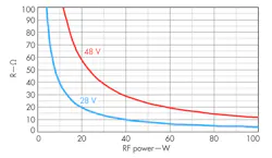
Figure 1 plots ROUT for both +28- and +48-VDC device operation across a typical output-power range. It shows how an amplifier designed for +28-VDC operation is well optimized for output-power levels of 8 to 10 W, requiring minimal impedance transformation for 50-Ω systems. It becomes obvious from Fig. 1 how +48-VDC operation is capable of nearly 25 W output power with minimal impedance matching needed for the same 50-Ω system compared to +28-VDC operation.
In addition to increased ROUT, +48-VDC operation also provides further benefits that can ease matching complexity. All things being equal, the usable bandwidth for an amplifier is fundamentally limited by the metrics of impedance transformation ratio and device quality factor (Q):
Impedance transformation ratio = Re(ZDEVICE)/50 Ω Device Q, where Q ≈ Im(ZDEVICE)/Re(ZDEVICE) and ZDEVICE ≈ ROUT + 1/jωCOUT (2)
The impact of these limitations varies with frequency, but there are general trends. With +28-VDC devices, the transformation ratio becomes the limiting factor—i.e., low ROUT tends to limit the available bandwidth. With +48-VDC devices, smaller COUT and larger ROUT mitigate both factors, and device Q tends to set the limit. Parameter COUT limits the usable maximum frequency in all cases.
This file type includes high resolution graphics and schematics when applicable.
Overcoming Limitations
This file type includes high resolution graphics and schematics when applicable.
A further complication arises at higher power levels—typically around 100 W device output power. At this level, ROUT and COUT for +28-VDC devices result in low output impedances that approach 2 Ω or less, making it difficult to achieve impedance matching for 50-Ω systems. A typical +28-VDC LDMOS device at 100 W adds an output impedance prematch to arm an amplifier designer with more reasonable terminal impedances. The added complexity increases the package size, however, nearly doubling the printed-circuit-board (PCB) area needed for a +28-VDC device for the same power level.
To simplify this problem for the sake of comparing +28- and +48-VDC devices—looking only at the resistance and capacitance characteristics of the amplifying die—it is possible to show that the available bandwidth for a given mismatch also follows the voltage ratio. A +48-VDC device will provide about 70% increased bandwidth potential compared to an equivalent powered +28-VDC device.
If the system requires only moderate bandwidth, there are still good reasons for using a +48-VDC solution. The lower Q or transformation ratio allows for more simplistic matching topologies since the load impedances require less transformation. These simplistic topologies also tend to be more resistant to manufacturing tolerances (i.e., PCB and matching component variations due to assembly).
For a realistic comparison, Table 2 shows fundamental properties for two similar 100-W GaN-on-Si devices, the +28-VDC model NPT1010 and +48-VDC model NPT2010 devices. Both devices use a 100-W die with no output impedance prematching and the same substrate thickness, die attach technique, and metal air cavity package. Among these measures, two differences stand out. The optimum load impedance of the +48-VDC device is significantly higher with the ratio of the real part at 3:1, consistent with theory.
The second obvious difference is thermal resistance (RθJC). This is the exception in the comparison of devices, whereby the smaller +48-VDC die can push performance in the wrong direction on account of more power being produced in a smaller area. Both devices are designed to operate with adequate margin to achieve rated output power levels below maximum rated junction temperatures for a given ambient condition. A significant thermal limitation for these high-power devices is the AC360 air-cavity flange package. The limitations of the package serve as a reminder of the need for more enhanced thermal packaging techniques to further enhance +48-VDC device operation.
In addition to enabling broader bandwidths, higher output impedances also enable alternative matching topologies, some of which were previously impractical. One of these, for example, is a broadband amplifier targeting 90 W output power from 100 MHz to 1 GHz. A ferrite-based impedance transformer is the best choice for a decade-plus bandwidth in the VHF/UHF bands; these topologies are ideally suited for N2:1 impedance ratios such as 1:1, 4:1, and 9:1.
From Eq. 1, an amplifier based on +28-VDC devices would require a load resistance of about 4.5 Ω, and 9:1 would be the ideal ratio for a transformation to 50 Ω. But a 9:1 impedance transformer is difficult to realize. The higher permeability materials needed to enable the low-frequency transformation become lossy at high frequencies, preventing full band coverage.1 Realistically, a high-power ferrite transformer with 9:1 transformation ratio will suffer from high loss and struggle to work above a few hundred MHz.
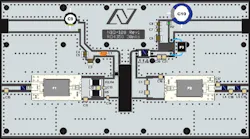
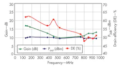
With a +48-VDC drain supply, the load resistance is much higher, nearly 12.5 Ω, and a lower-ratio 4:1 transformer is better suited to make the impedance transformation to 50 Ω. This lower transformer ratio is ideal for frequency coverage from 100 MHz to 1 GHz. With a nominal 100-W device, the simple and low-cost design shown in Fig. 2 delivers more than 80 W output power over the entire frequency band, achieving 50 to 70% efficiency with a single device. Figure 3 shows the efficiency performance for this design.
This file type includes high resolution graphics and schematics when applicable.
Achieving Balance
This file type includes high resolution graphics and schematics when applicable.
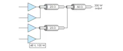
A balanced design (push-pull) amplifier configuration also benefits from higher output impedances. Two +48-VDC devices, each with 12.5-Ω load resistance at 90 W output power, present an impedance of 25 Ω to the primary in a push-pull configuration. Figure 4 shows how four devices can be set in a balanced push-pull configuration combined using coaxial sleeve baluns, allowing operation over a wide bandwidth.2 Higher output impedances enable other transmission-line transformer and combinational networks. Depending on the frequency band and required bandwidth, many tailored topologies are available for consideration.3
Power amplifiers (PAs) for wireless infrastructure applications with wideband-code-division-multiple-access (WCDMA), Long Term Evolution (LTE), orthogonal-frequency-division-multiplex OFDM, and other high-peak-to-average (PAR) waveforms face a real challenge. Achieving even modest amplifier efficiency is difficult when the RF amplifier is appropriately sized for peak power levels that are 8 to 10 dB higher than the average power level.
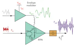
Envelope tracking (ET) is one of several effective techniques to address this issue. ET raises and lowers the drain voltage to follow the instantaneous peak amplitude of the device, effectively adjusting the compression point of the amplifier in real time to increase amplifier efficiency (Fig. 5). A peak-to-average ratio (PAR) of 10 dB, or 10×, implies a voltage ratio of approximately 3:1. This is a typical ratio seen in commercial systems.
For ET with +28-VDC devices, the drain supply typically varies between +10 and +30 VDC. This presents a problem for both GaN and LDMOS devices at the low end of this range because small-signal gain becomes nonlinear as a function of supply voltage. Above about +12 VDC, the gain increases linearly with voltage, but below +10 to +12 VDC, the gain enters a nonlinear region and can drop several dB below its nominal level at higher voltages. The statistical nature of a high-PAR signal implies an ET PA operates in this low-voltage region most of its time, thus encountering this unwelcome nonlinear gain condition. With a +48-VDC device, a typical ET system varies the drain between +20 and +60 VDC and the minimum voltage remains well above the onset of the nonlinear gain condition.
A +48-VDC GaN device provides an additional benefit over an LDMOS device because of the reduced COUT of the device. As mentioned previously, the higher COUT of LDMOS devices mandates internal pre-matching on the output to provide more friendly terminal impedances. The chosen topology for this output pre-match is usually a shunt-L match in the RF path. The shunt-L is designed to resonate with COUT to improve the terminal impedance.
All active transistor devices have terminal capacitances that vary versus applied voltage. When the drain supply voltage is modulated to follow the signal envelope, the drain-to-source capacitance (CDS) also varies and the shunt inductance (L) resonance is impacted, changing the terminal impedance of the device in real-time with the drain voltage. This leads to a nonoptimal impedance match for ET applications.5
In addition, because the shunt-L match requires a large shunt DC-blocking capacitor, there is additional strain on the envelope modulator design (Fig. 5), which is already challenged to swing large voltages with high current capability at high data bandwidths. The large blocking capacitor prevents the envelope modulator from being able to raise and lower the supply voltage in time with the modulation bandwidth. The low COUT of GaN devices means this matching topology is not needed, making +48-VDC GaN devices inherently optimized for ET applications.
A transition to a +48-VDC drain supply may raise concerns given the higher voltage. Although there may be thoughts that a higher voltage causes additional stress and lower reliability, this has not been found to be the case. Between +28 and +48 VDC, no difference has been found in DC reliability studies, with both voltage optimized technologies achieving 1 × 10⁶ hours mean time before failure (MTBF) at a junction temperature of +200°C. It is important for RF system design engineers to realize the connection between junction temperature and device reliability. The key to reliable design is maintaining device junction temperature below specified limits. Designers need to monitor ambient temperature and operating conditions (power dissipation) to guarantee reliable operation.6
Compared to +28-VDC devices, +48-VDC devices are physically smaller for a given RF power rating and the advantages of performance come primarily from this difference. This flows down into every aspect of the device, from the difficulty and performance of the impedance match, to the usable bandwidth and relative achievable performance.
Legacy commercial and military RF systems are well rooted in the use of +28-VDC power-amplifying devices. While LDMOS and GaN device suppliers will continue to support and increase +28-VDC offerings, new systems with the flexibility to do so should consider higher-voltage devices. The +48-VDC GaN-on-Si devices offer compelling advantages for those willing to consider this option.
Raymond A. Baker, Field Applications Engineer
Walter H. Nagy, Principal Engineer
David W. Runton, Vice President, Engineering
Robert A. Sadler, Principal RF Applications Engineer
Nitronex Corp., 523 Davis Dr., Ste. 500, Morrisville, NC 27560; (919) 807-9100, FAX: (919) 472-0692.
This file type includes high resolution graphics and schematics when applicable.
References
This file type includes high resolution graphics and schematics when applicable.
1. Jerry Sevick, Transmission Line Transformers, 4th ed., Scitech Publishing, Raleigh, NC, 2001.
2. Amin K. Ezzeddine and Ho C. Huang, “10-W Ultra-Broadband Power Amplifier,” IEEE MTT-S International Microwave Symposium Digest, 2008, pp. 643-646.
Related Articles
• GaN MMIC Amps Power 6 To 18 GHz
• GaN Switch Controls 20 GHz
• GaN Transistor Powers S-Band Radar
3. Chris Trask, “Designing Wide-band Transformers for HF and VHF Power Amplifiers,” QEX March/April 2005, pp. 3-15.
4. Jonmei J. Yan, Chin Hsia, Donald F. Kimball, and Peter M. Asbeck, “Design of a 4-W Envelope Tracking Power Amplifier With More Than One Octave Carrier Bandwidth,” IEEE Journal of Solid-State Circuits, Vol 47, No. 10, October 2012, pp. 2298-2308.
5. Jeffrey B. Shealy, Michael Lefevre, Bobby Anderson, David W. Runton, Matthew J. Poulton, and James Martin, “Optimization of gallium nitride high power technology for commercial and military applications,” Proceeding of Bipolar/BiCMOS Circuits and Technology Meeting, 2009. IEEE BCTM 2009.
6. “GaN Essentials, AN-012: Thermal Considerations for GaN Technology.”
This file type includes high resolution graphics and schematics when applicable.


