GaN HEMT Packs C-Band Power
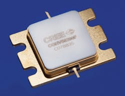
C-band communications systems both on the ground and in space rely on generous power to maintain their links. At one time, that signal power was from electron tubes, but now gallium nitride (GaN) high-electron-mobility-transistor (HEMT) active devices such as the model CGHV50200F from Cree can deliver tube-like power in packages that are a fraction of the size of electron tubes.
The model CGHV50200F HEMT may fit within a compact ceramic/metal flange package, but it provides 200 W typical continuous-wave (CW) output power from 4.4 to 5.0 GHz. It supports beyond-line-of-sight (BLOS) communications, satellite-communications (satcom), and troposcatter communications applications with high efficiency.
The flange-mount high-power GaN HEMT is internally matched to 50 Ω for ease of installation in many high-frequency circuits and subsystems. It is rated for typical saturated output power of 180 W from 4.4 to 5.0 GHz, with typical power gain of 11.5 dB and typical power-added efficiency (PAE) of 48% across that frequency range.
To give amplifier designers an idea of the performance levels possible in a typical circuit, Cree developed a demonstration amplifier and tested the performance for different parameters at different frequencies across the C-band operating range. The bill of materials (BOM) for this demonstration circuit is detailed on the data sheet for the GaN HEMT. It consists of standard circuit materials and passive circuit elements.
In this demonstration circuit, the model CGHV50200F GaN HEMT reaches CW output-power levels of 198 W at 4.4 GHz, 213 W at 4.6 GHz, 233 W at 4.8 GHz, and 218 W at 5.0 GHz. In the same circuit, it achieves small-signal gain of 14.9 dB at 4.4 GHz, 14.9 dB at 4.6 GHz, 14.9 dB at 4.8 GHz, and 15.1 dB at 5.0 GHz.
The power gain in the demonstration circuit, measured with orthogonal quadrature phase shift keying (OQPSK) modulation test signals, is 11.4 dB at 4.4 GHz, 11.6 dB at 4.6 GHz, 11.0 dB at 4.8 GHz, and 11.8 dB at 5.0 GHz. Since the evaluation circuit maintains a good 50-Ω match to the GaN HEMT, it provides high PAE of 49% at 4.4 GHz, 47% at 4.6 GHz, 48% at 4.8 GHz, and 48% at 5.0 GHz.
The flange-mount GaN HEMT is rated for maximum drain-to-source voltage of +125 VDC, maximum gate-to-source voltages of +10 and +2 VDC, maximum operating junction temperature of +225°C, maximum forward gate current of 41.6 mA, and maximum drain current of 17 A. The transistor has received an electrostatic discharge (ESD) classification of 1A (voltages greater than 250 V) for the human body model (HBM) and class 2 for the charge device model (CDM) (voltages from +125 to +250 V).
Cree, Inc., 4600 Silicon Dr., Durham, NC 27703; (919) 313-5300, FAX: (919) 869-2733

