RFICs Aim for Higher Functional Densities
This file type includes high resolution graphics and schematics when applicable.
Modern electronic products, such as cellular telephones and computers, continue to deliver increased functionality in smaller packages. Higher-density integrated circuits (ICs) are enabling this trend, while being designed for lower power consumption and increased efficiency. Advances in semiconductor processing, semiconductor materials, and device packaging all contribute to the “densification” of all IC types, which makes it possible to design and develop smaller circuits and smaller electronic products.
High-frequency ICs for RF and microwave applications are fabricated on a number of different substrate materials, including silicon wafers and III-V group compound semiconductor materials such as gallium arsenide (GaAs) and gallium nitride (GaN). GaAs has the high electron mobility to support high-frequency circuits well into the millimeter-wave frequency range (30 to 300 GHz), while GaN is a wide-bandgap material with high breakdown voltage and excellent high-power capabilities.
As with GaAs, GaN devices were initially developed for military/aerospace applications, such as solid-state radars and portable radio transmitters. But GaN-based ICs are becoming widespread for commercial applications, such as monolithic microwave integrated-circuit (MMIC) power amplifiers for wireless cellular base stations, and even at millimeter-wave frequencies as high as 77 GHz, in automotive collision-avoidance radar systems.
Going with GaN
The spread of GaN semiconductor technology in both discrete-device and IC forms has been rapid during the past few years, with semiconductor foundries worldwide exploring the material’s capabilities for high output power at high frequencies. Single-function MMICs such as power amplifiers and switches are available from a large number of suppliers, with some beginning to offer ICs that feature a combination of functions—e.g., switches and multistage amplifiers—on the same chip.
Silicon has been a semiconductor material of choice for many years, since it is a readily available material and inexpensive. As ICs moved higher in frequencies during the 1970s, however, the frequency limitations of devices fabricated on silicon substrates became apparent. Early U.S. Department of Defense (DoD) funding accelerated the development of GaAs substrate material for higher-frequency discrete devices and ICs. Along the way, additional compound semiconductor substrate materials, including indium phosphide (InP) or silicon germanium (SiGe) for high frequencies and silicon carbide (SiC) for high power, have been developed in different semiconductor foundries. That being said, GaN has become the current “material of interest” for a wide range of applications, from power supplies to RF/microwave devices and light-emitting diodes (LEDs).
Although ICs can be fabricated on pure GaN wafers, more often than not, the GaN layers are formed on a backing layer (such as GaN-on-Si or GaN-on-SiC) to leverage some benefit from the second material—e.g., the low cost of silicon or the excellent thermal properties of SiC. Thermal management is a key concern when striving for higher levels of integration with GaN-based semiconductors. The high power density of GaN discrete devices and ICs results in large temperature rises in small areas.
Applications that require high power levels even in peak form, such as pulsed phased-array radars with multiple amplifiers, are being made more compact, although the heat generated by the active GaN devices must be effectively managed. Even the most efficient GaN amplifiers will generate heat that must be effectively dissipated to maintain IC performance and preserve reliability.
Developers working with GaN-on-Si and GaN-on-SiC processes are exploring the thermal issues, especially for semiconductor processes capable of minute device features. Semiconductor foundries often offer fabrication services for multiple substrate materials like GaAs and GaN, although the GaN process will be either on Si or SiC. Many commercial foundries focus on GaN-on-SiC fabrication services due to the excellent thermal properties of the SiC substrate material. These include Wolfspeed, HRL Laboratories, United Monolithic Semiconductors (UMS), Qorvo, and WIN Semiconductors.
Some foundries offering GaN IC fabrication services may not be as well known, such as defense contractors BAE Systems and Northrop Grumman. The latter runs a semiconductor foundry in Redondo Beach, Calif., for both commercial and military/aerospace customers. This is a foundry with processes in GaAs (to 100 GHz), GaN (to 60 GHz), and InP that fabricates devices to frequencies as high as 140 GHz. The InP processes feature both 0.1-μm high electron mobility transistors (HEMTs) and heterojunction bipolar transistors (HBTs).
One attractive feature of GaN-on-Si semiconductor processes has been their low cost and the opportunities to apply the benefits of GaN outside of RF/microwave designs. GaN transistors are noted for their low on-state resistance and low parasitic capacitance, characteristics that enable fast switching speeds when used in power supplies.
Navitas Semiconductor, for example, has focused on energy applications for GaN and developing GaN ICs for power control and supplies. GaN Systems has applied HEMTs fabricated with GaN-on-Si technology to power electronics, such as dc-dc converters with fast switching speeds. Infineon Technologies has explored a variety of applications for GaN ICs, from audio amplifiers to microwave switching. Efficient Power Conversion also uses GaN devices for audio amplifiers. GaN-on-Si processes have been employed for high power lasers, as well as light-emitting diodes to enhance brightness versus LEDs fabricated on Si substrates.
GaN-based ICs are growing smaller over time, even as suppliers learn to handle thermal issues while cutting product costs. Though GaN MMIC amplifiers, for example, are still available from many suppliers in ceramic packages with excellent thermal conductivity to effectively dissipate heat from the GaN ICs, a growing number of GaN MMIC amplifiers are now available in lower-cost plastic packages. Nevertheless, users are advised to ensure that adequate heat-sinking is provided around the device at the circuit level.
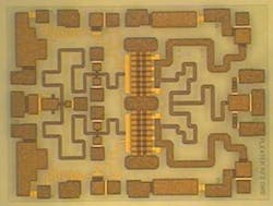
Smaller die sizes promote more compact circuit designs and the opportunity to supply the ICs in smaller packages. The smaller die sizes also bring economic benefits for semiconductor suppliers. As researchers at Plextek RFI discovered when developing a GaN MMIC power amplifier for X-band radar applications (Fig. 1), high power was possible even in extremely small die size.
The GaN HEMT amplifier MMIC (see Stuart Glynn and Liam Devlin, “An X-Band GaN PA MMIC for Phased Array Radar Applications," ) was fabricated at WIN Semiconductors using a 0.25-µm gate-length process, resulting in a GaN MMIC amplifier die measuring just 1.5 × 2.5 mm. In addition to meeting a customer’s need for high output power of 25 W output power from 10 to 12 GHz in a small size for phased-array radars requiring multiple channels of amplification, many amplifiers were produced per wafer. For the 4-in. GaN-on-SiC wafers used at the time of the work, about 2,300 amplifiers were fabricated per wafer.
Of course, GaN MMICs have some ways to go to match the levels of integration available in high-frequency silicon CMOS ICs, or even GaAs MMICs for that matter. But growing demands for wireless communications services and equipment with higher data rates, and the loads that are expected to be placed on wireless networks by new applications—such as Internet of Things (IoT) devices using wireless links to access the Internet and wirelessly connected motor vehicles—is driving chip designers to find ways to pack more functionality into less semiconductor space.
While digital IC designers have almost routinely achieved high circuit densities in their ICs, the design constraints of RF/microwave ICs often throw roadblocks in the way of RF chip designers seeking to shrink the size of their ICs. These challenges include the importance of impedance matching and providing sufficient isolation between multiple on-chip signal sources; among these are oscillators and component functions with low-level sensitivities, e.g., low-noise amplifiers (LNAs).
Nonetheless, the design team for the ADR6612 and ADR6614 ICs from Analog Devices deserve much credit for their accomplishments of fabricating complete radio receivers and transmitters with multiple LOs for frequencies from 0.7 to 3.0 GHz on one chip. Although the transceivers are not sold in die (chip) form, they are small enough to fit within 48-lead LFCSP housings that measure just 7 × 7 mm. The implications of this level of integration are significant, especially for systems that must provide functionality while remaining physically “unnoticeable,” such as for in-building microcells to provide wireless communications coverage in offices, malls, and other enclosed spaces.
Silicon RF/microwave ICs will not be quickly forgotten. As Peregrine Semiconductor recently demonstrated, silicon CMOS technology is not close to reaching its top frequency. The firm recently announced the latest generation of its silicon-on-insulator (SOI) technology with low on-resistance and off-capacitance for a transition time of 80 fs.
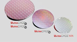
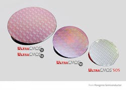
The UltraCMOS 12 process (Fig. 2), developed in conjunction with foundry Global Foundries, fabricates devices on 300-mm-diameter SOI wafers for relatively high yields. The process is able to fabricate ICs well into the upper reaches of the millimeter-wave frequency range, in support of emerging applications such as 5G wireless communications and automotive radar systems.
This file type includes high resolution graphics and schematics when applicable.


