How to Select the Right Data Converters
Data is essential to any military defense system, and handling data efficiently usually is the task of a handful of key components. But perhaps no components are more important in an advanced signal-processing system than its analog-to-digital converters (ADCs) and digital-to-analog converters (DACs), which cannot afford to fail or even be slightly in error.
Suppliers of ADCs and DACs have made impressive advances regarding processing power for power consumed in these components over recent years, and troops around the world (and sometimes in space) rely heavily on the performance of these components in stationary and portable systems. Often, finding the right data converter for a system design is simply a matter of understanding the relevance of different data-converter specifications and which of those are the most important for an application.
ADCs and DACs are typically used in systems with signal amplifiers, filters, digital signal processors (DSPs), and other components to help with the extraction of information from processed signals. Typically, data converters are specified first in a system design, setting the performance limits for that system (and the requirements for many of the system’s other components). By placing the ADCs as close to the antennas as possible, for example, the antenna’s dynamic and frequency ranges can be digitized quickly by the ADCs for analysis in the digital realm.
Many defense-based systems are designed for portability, such as software-defined radios (SDRs), for applications driven by designs that require minimal power consumption for extended operating periods on battery power. The rechargeable battery is part of the portability and must be as small and light in weight as possible while still providing the energy requirements of an SDR’s various components, including ADCs and DACs.
Sampling ADCs
One fundamental requirement when choosing an ADC is determined by the frequency of the analog input signal to be processed. According to Nyquist sampling theory, the signal to be digitized should be sampled at a speed that’s more than two times the analog frequency, with higher sampling rates providing greater details about the signal to be sampled. Those higher sampling rates usually come with higher ADC power requirements, however, resulting in the need to weigh a set of data-converter performance parameters when trying to also achieve extended operating times on battery power.
Nyquist theory is based on sampling repeatable signals, such as sinewaves without deviations or modulation. The more irregularities in the signal to be sampled, the greater the need for an ADC with a higher sampling rate to capture any deviations in the signal flow. Additional components, such as anti-aliasing filters, can help achieve effective digitization of input signals when the available ADC sampling rate may be considered low for the signals to be sampled.
Selecting an ADC for any system application is a matter of weighing the different ADC performance parameters versus the requirements of the application, such as power consumption in a portable radio and a high sampling rate for a high-frequency application. The bit resolution of an ADC can be critical to some applications, such as for a radar onboard a ship or aircraft that must be capable of discerning a small weapon (e.g., a missile) against a much larger background.
Higher bit resolution will be needed to separate irregularities in processed pulses, such as the delays and amplitudes of pulses reflected from a jet aircraft compared to the pulses returning to a radar receiver from a jet-fired missile. As with many other ADC performance parameters, though, high-resolution ADCs like 20-b converters typically provide much lower sampling rates than that available with lower-resolution ADCs, such as 8-b converters.
When comparing different model ADCs from Texas Instruments (www.ti.com), for example, greater bit resolution means lower sampling-rate speeds. For a bit resolution of 16 b, for example, the highest-speed ADC operates at 200 Msamples/s. For slightly less bit resolution of 14 b, the firm’s best ADC operates at a top sampling rate of 400 Msamples/s. This trend of decreasing bit resolution for increasing sampling rate follows for other TI ADCs, with a 12-b ADC providing up to 2-Gsample/s rates and its fastest 8-b ADC operating at 3-Gsample/s or better sampling rates.
These ADCs are typical of the trends found in bit resolution versus sampling rates. In addition, higher numbers for both specifications usually mean higher power consumption for an ADC compared to a component with lower bit resolution and sampling rates.
For many systems, noise performance is important; an ADC’s datasheet will provide information on a converter’s signal-to-noise ratio (SNR) and its total harmonic distortion (THD). High values indicate a converter that can detect small or weak signals in the presence of interfering signals and/or noise, transforming input signals into meaningful code for processing by the other components in the system, such as DACs and digital signal processors (DSPs).
Aperture jitter or uncertainty is another ADC noise parameter, a measure of the sample-to-sample variations in aperture delay, typically measured in piscoseconds root mean square (RMS). It may appear as frequency-dependent noise on an ADC’s input port and can convert to phase noise within a system; thus, it should be minimized.
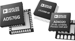
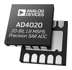
Many converter suppliers, including Analog Devices, have developed functions and features to conserve ADC power. High-resolution ADCs such as the 20-b AD4020 (Fig. 1) are designed to save power where possible; for example, using fully differential input ports and a high-impedance mode so that the ADC can be driven directly with lower-power precision amplifiers. The ADC also operates with a low serial peripheral interface (SPI) clock-rate requirement for reduced power consumption. The AD4020 runs from a +1.8-V dc supply and achieves relatively high processing speeds, at 1.8 Msamples/s, but only consumes 15 mW power at its maximum rated sampling speed and less power at lower sampling speeds.
1. Model AD4020 is an example of a high-resolution ADC, at 20 bits. It samples analog input signals at 1.8 Msamples/s, but only consumes 15 mW from a +1.8-V dc supply at the maximum sampling rate. (Courtesy of Analog Devices)
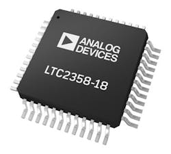
The model LTC2358-18 from Linear Technology, now part of Analog Devices (Fig. 2), simultaneously samples on eight channels with as much as 200-ksample/s throughput per channel. It has differential inputs and an internal clock to minimize latency in the sampling cycles and guarantees 18-b resolution, with no missing codes.
2. To save power and size, ADCs such as the model LTC2358-18 from Linear Technology/Analog Devices pack eight channels, each with its own ADC, within a miniature package that has many supporting components. (Courtesy of Analog Devices)
In terms of functionality, the LTC2358-18 is an example of a densely packed device well-suited to the audio range. Replete with an integrated reference source and buffer amplifier, it’s capable of a typical 96.4-dB single-conversion SNR. When working with audio signals, the ADC features THD of typically −111 dB for a 2-kHz input signal. It includes SPI CMOS and LVDS serial input/output (I/O) interfaces for ease of control interconnections, using a 7- × 7-mm LQFP package with 48 leads for connections to the SPI CMOS and LVDS serial interfaces.
Return to Analog
On the other side of the system, DACs provide the reverse functionality of an ADC to return digital representations of signals to analog form. For most receivers, a set of DACs will provide almost “mirror-image” functionality and performance to that of its ADC cousins, converting code with the same bit resolution and sampling rates. For instance, the tradeoffs in power consumption and performance typical of ADCs are also present for DACs and should be weighed against system requirements as well as for compatibility with the ADCs in a system. Depending on the system design, DACs can provide low- or high-voltage outputs, with single-voltage outputs for simpler designs, multiplying outputs for higher-frequency configurations, and current-output devices when required.
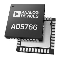
As an example, the AD5766 and AD5767 denseDACs from Analog Devices are 16-channel, 16- and 12-bit DACs that are highly integrated with supporting components, including reference buffer amplifiers, multiplexers, and channel-monitoring multiplexers (Fig. 3). Incorporating 16 independent DACs within each package, they are compatible with 1.8-V logic and generate analog output voltages from an external 2.5-V reference.
3.When moving from digital code back to analog signals, converters such as the AD5766 and AD5767 denseDACs provide 16 channels of processing with high resolution by means of 16 separate DACs within a small package. (Courtesy of Analog Devices)
Both devices are available within either of two compact housings: a 4- × 4-mm, 48-lead WLCSP and a 6- × 6-mm 40-lead LFCSP. The DACs feature eight software-programmable output ranges, including −20 to 0 V, −16 to +10 V, and ±5 and ±10 V, and integrated DAC output buffers capable of ±20 mA current. The operating temperature ranges for both DACs is −40 to +105°C.
This brief rundown of some readily available ADCs and DACs provides a “sampling” of how the specifications change depending on specific requirements. For example, higher resolution is available for lower frequencies, along with impressive integration of multiple components to achieve many channels within a multipin or multiple-lead surface-mount-technology (SMT) package. While no single ADC or DAC provides the ultimate performance levels that can satisfy all system requirements, smart selections can be made by using the most critical requirements of a system, such as size, power, or resolution, to help guide the choice.


