Load-Pull Analysis with Software Enables Wave of Designs
This file type includes high resolution graphics and schematics when applicable.
Load-pull analysis is an important aspect of the design process of an amplifier, as this technique is often used to determine an appropriate load. Thus, by utilizing load-pull techniques, amplifiers can be designed more efficiently. In the application note, "Load-Pull Analysis Using NI AWR Software," National Instruments presents three design examples that take advantage of the load-pull technique. These designs are aided with the NI AWR Design Environment.
The first example demonstrates a simple load-pull analysis. The impedances that were obtained are presented on the Smith Chart. Additional graphs display saved data sets of measured output power versus gain compression, output power versus power-added efficiency (PAE), and input power versus output power. By taking advantage of the capabilities of the NI AWR software, designers can quickly learn the impact of load/source terminations on an amplifier’s performance over swept input power. Power amplifier (PA) designers can therefore gain a better understanding of the tradeoffs between load impedance and gain compression behavior.
In the next example, a device was terminated in a matching network based on a microstrip transmission line transformer. The impedances that were obtained are once again displayed on the Smith Chart. Contour lines on the Smith Chart indicate where +45 dBm of output power and 70% PAE can be attained, respectively. The layout of the matching circuit is presented, as well as the performance characteristics of the device with the matching network.
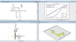
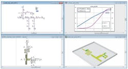
The third example investigates circuit optimization by means of electromagnetic (EM) field analysis. By leveraging EM analysis, a more accurate representation of the matching network impedance can be achieved. Although EM analysis is often used in design verifications after the final design has been achieved, this example illustrates the accuracy of EM analysis when used earlier in the design process. The schematic and layout of the final project is presented. The output matching circuit for the transistor model was also created based on the measured load-pull file to investigate the current distribution through the matching structure.
National Instruments Corp., 11500 N Mopac Expwy., Austin, TX 78759-3504; (877) 388-1952
Looking for parts? Go to SourceESB.
This file type includes high resolution graphics and schematics when applicable.


