Dive into EM/Circuit Co-Simulation of a T/R Front-End Module and Actively-Scanned Array, Part 2 (.PDF Download)
5G is poised to bring more integrated and sophisticated antenna and circuit modules to the modern defense and commercial electronics markets. Part one of this article examined today’s multi-technology circuit and electromagnetic (EM) simulation challenges and the software tools needed to support the successful design of 5G products.
Part two presents examples that illustrate the use of multi-technology in an EM simulation and EM/circuit co-simulation of an actively-scanned antenna array. Advanced technologies such as parameterized 3D cells, shape pre-processing and simplification, 3D EM extraction, and in-situ measurements are described.
Example: Multi-Technology RFIC/MMIC Package on Board
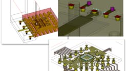
In this case, we’ll illustrate the use of multi-technology in an EM simulation. The area of interest is the launch from the board onto the package and then onto the chip within the package (Fig. 1). The board uses a printed-circuit-board (PCB) library. The device package utilized is quad, flat, no-leads (QFN).
1. Shown is an RFIC/MMIC in a QFN/flip-chip/wire-bonding package on a PCB.
The package is connected to the chip by means of bond wires. Three libraries are used in this example, one each for the board, package, and chip layout cells. The designer is interested in answering questions about the performance of the launch, grounding issues, package resonances, layout optimization, and performing yield analysis for manufacturability issues.


