5G Front-End Reference Design Meets Multiple Needs

5G Front-End Reference Design Meets Multiple Needs

July 13, 2018
Integrating a power amplifier, a pre-driver amplifier, and a receiver switch/low-noise amplifier, this flexible front-end solution is equipped for next-generation 5G communications.

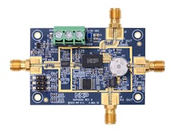
Without question, 5G communications was a central theme at IMS 2018. One standout 5G-based product at the show was NXP Semiconductors’ new RF front-end reference design for 5G massive multiple-input, multiple-output (MIMO) systems (see figure). This front-end solution supports frequencies ranging from 2.3 to 5.0 GHz. Furthermore, it integrates a combination of silicon-germanium (SiGe), gallium-arsenide (GaAs), and laterally diffused metal-oxide semiconductor (LDMOS) technologies.

The functionality of the front-end solution is the product of three main components. One is an LDMOS Doherty power amplifier module (PAM). NXP offers different PAM variants that are all footprint-/pin-compatible, meaning any PAM version can be mounted onto the reference design board.

The second component is a low-power Doherty pre-driver amplifier module. Like the PAMs, NXP offers different footprint-/pin-compatible pre-driver amplifier versions, so that each one be incorporated into the reference design. The third component is a receiver front-end module, which is comprised of a transmit/receive (T/R) switch and low-noise amplifier (LNA).

This new RF front-end reference design for 5G massive-MIMO systems supports frequencies from 2.3 to 5.0 GHz.

With the footprint-/pin-compatible PAMs and pre-driver amplifiers, customers can essentially “plug-and-play” among different frequencies and power levels, as the same board design can accommodate different component versions. The PAM versions each cover various frequencies and power levels, while the pre-driver amplifier versions handle different frequency bands. Moreover, the front-end solution requires fewer components on a printed-circuit board (PCB), which reduces total system costs. NXP also notes that a significant benefit of the design is its small size—the front-end assembly measures about 21 × 35 mm.

The PAMs, which are based on LDMOS technology, come in packages that measures 6 × 10 mm. Their output power level ranges from 2.5 to 5 W. In addition, the input and output of the components are both matched to 50 Ω.

The pre-driver amplifiers, offering 32 dB of gain, are housed in a 3- × 4-mm package. The amplifiers achieve a 1-dB compression (P1dB) of either +25 or +29 dBm, depending on the supply voltage (the amplifiers require either +3.3 or +5 V; Id is 50 mA). Like the PAMs, the input and output of the pre-driver amplifiers are matched to 50 Ω.

Lastly, as mentioned, the receiver front-end module comprises a T/R switch and LNA. It comes in a 4- × 4-mm package. Covering the full frequency range of 2.3 to 5.0 GHz, the receiver front-end module provides about 33 dB of gain while achieving a noise figure of less than 1.2 dB. Its switching speed is 0.8 µs. Operating from a 5-V supply, the component’s current consumption is 100 mA. Like the PAMs and pre-driver amplifiers, the input and output of the receiver front-end module are both matched to 50 Ω.

Sponsored Recommendations

Phase Noise Fundamentals: What You Need to Know

Dec. 26, 2024
Gain a deeper understanding of phase noise and its impact on oscillators. This white paper offers a concise technical introduction to phase noise concepts, along with an overview...

Selecting Your Next Oscilloscope: Why Fast Update Rate Matters

Dec. 26, 2024
Selecting your next oscilloscope - A guide from Rohde & Schwarz

Webinar: Fundamentals of EMI Debugging & Precompliance

Dec. 26, 2024
In this webinar our expert will guide you through the fundamentals of EMI debugging & precompliance measurements.

Learn the Fundamentals of Test and Measurement

Dec. 26, 2024
Unlock your measurement potential with Testing Fundamentals from Rohde & Schwarz. Expert resources to help you master measurement basics. Explore now.