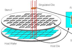
Stacked, three-dimensional (3D) integrated circuits (ICs) promise a great deal of electronic functionality in tight spaces, but they also challenge the best capabilities of the test-and-measurement companies to characterize these devices. Rising to that challenge, wafer probe specialist Cascade Microtech and top nanoelectronic research center imec have teamed to develop solutions for proving 3D ICs to the level of 25-micron-diameter microbumps. By means of a Joint Development Agreement, Cascade partnered with imec to characterize a test wafer with its automated model CM300 probe station with an advanced version of its Pyramid Probe® technology. The 3D semiconductor market is expected to grow rapidly in the coming years, supporting markets in computing, defense, and medical fields.
About the Author
Jack Browne
Technical Contributor
Jack Browne, Technical Contributor, has worked in technical publishing for over 30 years. He managed the content and production of three technical journals while at the American Institute of Physics, including Medical Physics and the Journal of Vacuum Science & Technology. He has been a Publisher and Editor for Penton Media, started the firm’s Wireless Symposium & Exhibition trade show in 1993, and currently serves as Technical Contributor for that company's Microwaves & RF magazine. Browne, who holds a BS in Mathematics from City College of New York and BA degrees in English and Philosophy from Fordham University, is a member of the IEEE.
