This file type includes high resolution graphics and schematics when applicable.
Lowpass filters (LPFs) are invaluable in communications and other electronic systems for their capabilities to screen out higher-order interference and noise. To achieve a 1.8-GHz microstrip LPF in a relatively small size, a unit was designed with quasi-Yagi defected ground structure (DGS) and compensated capacitors. It achieved a sharp cutoff frequency response with low passband insertion loss and wide rejection band, with about 20-dB attenuation from 2.8 to 11.0 GHz. With the aid of Microwave Office circuit simulation software from AWR Corp., an equivalent-circuit model was derived and circuit parameters were extracted using a simple circuit-analysis method. The rejection band can be adjusted by controlling the dimensions of the Yagi structure. A prototype of the filter fabricated on commercial printed-circuit-board (PCB) material measured just 0.45λg x 0.35λg, with 0.45λg = 44 mm.
Related Articles
• Compensating For DGS Filter Loss
• Antenna Aims At Dual Bands
• Programmable LPF Screens ADC Circuits
Circuit designers have been discovering the usefulness of defected microstrip structures (DMSs) and defected ground structures (DGSs) in planar topologies, along with the added benefits of their relatively inexpensive fabricating using photolithographic techniques or PCB technologies.1,2 Periodic or nonperiodic DGSs can achieve good rejection at high frequencies, making it possible to reject undesired spurious and harmonic responses in microwave circuits.2,3
A DGS with a simple geometry (such as a rectangular shape) or a more complicated shape can improve the rejection band of a LPF.1,2 Typically, DGS units are used to design and improve filters,1 patch antennas,3,4 branch line couplers, power dividers, and power amplifiers.5 One technique for realizing DGSs is to etch a few defect patterns in the backside metallic ground plane of a PCB under a microstrip transmission line. The defect patterns disturb the shield current distribution in the ground plane, modifying the transmission-line characteristics of the microstrip (an increase in the effective inductance and capacitance) and achieving a slow-wave effect with bandstop properties.
Based on previous work using rectangular DGSs,6-17 a rectangular DGS with arms along the slot channel—essentially a quasi-Yagi DGS—was used to control the coupling between the cascaded resonators to improve the rejection-band response, reduce passband loss, increase the sharpness of the transition domain, and thus minimize the size of the filter structure. Four tuning stubs were added to the lowpass filter to create a wide rejection band and low passband insertion loss. Measurements performed on a fabricated filter show close agreement with simulations.
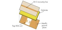
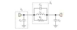
Figure 1 shows a three-dimensional (3D) view of the quasi-Yagi DGS unit, which consists of two rectangular heads, connected through horizontal and vertical thin slot-channels (arms) in the ground plane. Figure 2 shows a lossless equivalent-circuit model of the quasi-DGS unit, based on a Chebyshev π-network, where Cs represents the sum of the capacitances in the ground plane and Ls is the parallel inductance to Cs. The parallel capacitance, Cp, between the microstrip feed and the metallic plane is formed by the influence of the fringing field around the DGS unit. Resistance Rs accounts for radiation loss as well as loss from the dielectric substrate in the PCB material.
Calculating The Parameters
A circuit model was created with the help of Microwave Office. The equivalent-circuit parameters can be calculated from the S-parameters based on an electromagnetic (EM) simulation. Once the S21 and S11 parameters have been computed at the resonant frequency by the AWR simulator, the required circuit parameters can be defined by using the relationship between the S-ABCD patameters and the Y-parameters as described by the following equations:
A = [(1 + S11)(1 - S22) + S12S21]/2S21 = 1 +Yp/Ys (1)
B = [(1 + S11)(1 + S22) - S12S21]/2S21 = 1/Ys (2)
C = (1/Z0)[(1 - S11)(1 - S22) - S12S21]/2S21 = 2Yp + (Y2p/Ys) (3)
D = (1/Z0)[(1 - S11)(1 + S22) + S12S21]/2S21 = 1 + (Yp/Ys) (4)
where:
Ys = the series admittance of the π equivalent circuit;
Yp = the parallel admittance of the π equivalent circuit; and
Z0 = the characteristic impedance of the transmission line;
and
Ys = 1/Zs = 1/B (5)
Ys = 1/Zs = B = RsZLC/( Rs + ZLC), Rs = → ∞ (6)
Zs = ZLC = [(jωLs)(1/ jωCs)]/[jωLs + (1/jωCs)] (7)
Zs = ZLC = jωLs/[1 - ω2LsCs] (8)
YLC = [1 - ω2L3C3]/jωLs = j(ωCs – 1/ωLs) = jBLC (9)
BLC|ω = ωc = ω0Cs[(ωc/ω0) - ω0/ωc] (10)
Cs = BLC/ω0[(ωc/ω0) - ω0/ωc] and Ls = 1/(ω02Cs) (11)
Yp = (A - 1)/B = 1/Rp + jBRC ≈ jBRC = jωCp 12)
ω = ωc → Cp = BRC/ωc (13)
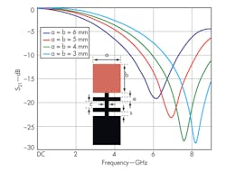
Figure 3 shows some of the electrical properties (resonance and cut-off frequencies) for changes in the length and width of the DGS head. The square head and its area (a x b) represents inductance, while the slots and distances between them (c, d) form capacitances. Values for the cutoff frequency, fc, and resonant frequency, f0, can be found from the transmission characteristics of the quasi-Yagi slot.6,7 The dimensions of the DGS (a = 8 mm, b = 3 mm, e = 1 mm, c = 2.5 mm, and s = 2.5 mm) were computed and optimized with the aid of the Microwave Office and Tex-line software packages.
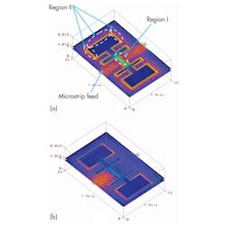
To verify the dependence of the equivalent-circuit elements (capacitance and inductance) on the PCB surface as part of the distribution EM field, EM simulations were performed with results shown in Figs. 4(a) and (b). For this analysis, the microstrip structure was divided into two regions. In region I, the electric field is highly concentrated in the gap, hence any change in the gap’s dimensions affects the effective capacitance of the structure. In region II, the electric field nearly vanishes. On the other hand, the current is distributed throughout the whole structure. Therefore, any change in the length of the square area strongly affects the magnetic field distribution and, hence, the surface current. This in turn leads to a change in the effective inductance of the structure. Therefore, region I corresponds to capacitance and region II corresponds to inductance. The full structure corresponds to an LC resonator.
This file type includes high resolution graphics and schematics when applicable.
A Closer Look
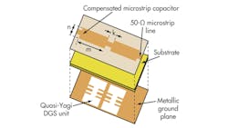
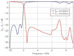
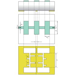
Figure 5 provides a schematic view of the DGS lowpass filter, which is comprised of two quasi-Yagi slots in the PCB’s metallic ground plane and two compensated microstrip capacitors,which are placed on the top layer and connected together by means of a 50-Ω feed line on the top circuit layer. To perform a computer-aided-engineering (CAE) software simulation, a four-pole LPF was simulated on RO4003 PCB material from Rogers Corp. with relative dielectric constant, εr, of 3.38 at 10 GHz in the material’s z-axis; a material thickness of 0.813 mm was used in the simulation. Figure 6 shows simulation results with Microwave Office. The dimensions for the compensation capacitors were calculated as m = 8 mm, n = 5 mm, and k = 4 mm.
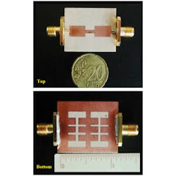
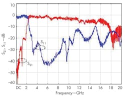
The optimized quasi-DGS-unit was used to design a LPF, fabricated on substrate measuring 30 x 20 mm2 with εr = 3.38 and thickness (h) of 0.813 mm. Figure 7 shows a photograph of the fabricated structure. Measurements were carried out on a model HP8719D RF/microwave vector network analyzer (VNA) from Hewlett-Packard/Agilent Technologies and are shown in Fig. 8. The fabricated LPF has a 3-dB cutoff frequency at 2 GHz and out-of-band rejection of 20 dB from 3 to 11 GHz; insertion loss in the passband is only about 0.65 dB. Figure 8 shows good agreement between the measured and simulated results.
This file type includes high resolution graphics and schematics when applicable.
Modeling Considerations
To improve the stopband frequency response of the filter, the DGS resonators were modeled and simulated with Microwave Office. Variations in the length of the horizontal arm (l) will shift the cutoff frequency and the attenuation pole location in the frequency domain. To understand the effects of changing the length of the horizontal arm, other dimensions of the structure were kept constant while the length (l) of the arms was varied (Fig. 9); simulation results are shown in Fig. 10. Decreasing the arm length resulted in decreasing the total capacitance, with the attenuation pole location moving to a lower frequency, and clear improvements in the reject-band response and sharpness of the cutoff-frequency response. The filter’s dimensions (w0 = 1.92 mm; w1 = 8 mm; w3 = 3 mm; h = 10 mm; l = 2 mm; and t = 2 mm) were computed and optimized with the aid of Microwave Office and Tex-line.
A meandered feedline has been used to previously to meet requirements for a compact polynomial five-deg. LPF with a quasi-elliptic approach and to also improve its rejection-band response (see Fig. 11). Addition of the meander line increases the inductance of the structure, which shifts the pole frequency to a lower-frequency range. Figure 12 shows strong suppression of the S21 response at higher frequencies, indicating that this modified resonator/filter topology affects the rejection band without any modifications in the size of the structure.
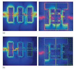
Figure 13 shows simulated EM field distributions for the DGS LPF in the stopband and passband. In the stopband at the 2-GHz (transmission zero) pole frequency, maximal magnet current concentrates around the first resonator, indicating that energy is not transferred to the output. As a result, the filter provides a stopband response [see Fig. 13(a)]. In the passband at the reflection zero of 1.2 GHz, almost all RF power passes through the filter structure. Maximum current concentration can also be observed on the metal stubs as well as on the microstrip line section between the three compensating capacitances on the top layer, which are coupled with both DGS resonators in the ground plane [see Fig. 13(b)].
This file type includes high resolution graphics and schematics when applicable.
Conclusions And References
Related Articles
• Compensating For DGS Filter Loss
• Antenna Aims At Dual Bands
• Programmable LPF Screens ADC Circuits
In summary, a new quasi-Yagi DGS LPF was developed and offers excellent performance both within its passband and throughout its stopband. The use of a meander feedline helps improve passband and stopband performance compared to a filter without the meander feedline. The novel quasi-Yagi resonator made it easier to control resonant frequency without extra devices, contributing to the compact size of the filter structure. In validation of the design approach used for the quasi-Yagi LPF, the measured results agreed closely with computer simulations of the filter’s performance.
Ahmed Boutejdar, Engineer
Abbas Omar, Engineer
Edmund Burte, Engineer
Microwave and Communication Engineering Institute, University of Magdeburg, Magdeburg, 39106, Germany.
Acknowledgments
The authors wish to thank the German Research Society (DFG) for financial support. The authors are also grateful to Microwaves & RF Technical Contributor Jack Browne for his assistance and cooperation, and to Mr. Harald Dempewolf, Laboratory Manager of the Institute for Electronics, Signal Processing, and Communication (IESK) at the University of Magdeburg, Germany, for his help and support.
References
1. A. Dal, J.S. Park, C.S. Kim, J. Kim, Y. Qian, and T. Itoh, “A design of the low-pass filter using the novel microstrip defected ground structure,” IEEE Transactions on Microwave Theory & Techniques, Vol. 49, May 2001, pp. 86-93.
2. A. Boutejdar, A. Batmanov, A. Elsherbini, A.S. Omar, and E. Burte, “Design of Compact Tunable Band-Pass Filter Using J-Inverter and Quasi-Fractal Defected Ground Structure (DGS),” Proceedings of the EUROEM European Electromagnetic 2008, Lausanne, Switzerland, July 21-25, 2008.
3. J.S. Kuo and K.L. Wong, “A Compact Microstrip Antenna with Meandering Slots in the Ground Plane,” Microwave and Optical Technology Letters, Vol. 29, No. 2, April 20 2001, pp. 95-97.
4. H. Liu, Z. Li, and J. Mao, “Harmonic suppression with photonic bandgap and DGS for a microstrip patch antenna,” IEEE Microwave & Wireless Components Letters, Vol. 15, No. 2, February 2005, pp. 55-56.
5. J.-S. Lim, H.-S. Kim, J.S. Park, and S. Nam, “A power amplifier with efficiency improved using defected ground structure,” IEEE Microwave & Wireless Components Letters, Vol. 11, No. 4, April 2001, pp. 170-172.
6. A. Boutejdar, M. Makkey, A. Elsherbini, and A. Omar, “Design of compact stop-band extended microstrip low-pass filters by employing mutual coupled square shaped defected ground structures,” Microwave & Optical Technology Letters, Vol 50, No. 4, April 2008, pp. 1107-1111.
7. A. Boutejdar, A. Rahman, A. Batmanov, A. Omar, and E. Burte, “Miniaturized Band-Stop Filter Based on Multilayer- Technique and New Coupled Octagonal DGS With Interdigital Capacitor,” Microwave & Optical Technology Letters, Vol.52, No. 3, March 2010, pp. 510-514.
8. C. Kim, J.S. Park, A. Dal, and J. Kim, “A novel 1-D periodic defected ground structure for planar circuits,” IEEE Microwave Guided Wave Letters, Vol. 10, April 2000, pp. 131-133.
9. A. Boutejdar, A. Batmanov, and A.S. Omar, “A compact bandstop/bandpass filter using a narrow gap capacitive as j-inverter and new octagonal defected ground structure,” 3rd European Conference on Antennas and Propagation, EuCAP 2009, March 2009, Berlin, Germany.
10. Ahmed Boutejdar, Anatoly Batmanov, Abbas Omar, and Edmund P. Burte, “A miniature 3.1 GHz microstrip bandpass filter with suppression of spurious harmonics using multilayer technique and defected ground structure open-loop ring," (book chapter), in Ultrawideband, Short-Pulse Electromagnetics, Springer, New York, 2010, ISBN: 978-0-387-77844-0.
11. A. Abdel-Rahman, A.K. Verma, A. Boutejdar, and A.S. Omar, “Compact stub type microstrip bandpass filter using defected ground plane,” IEEE Microwave & Wireless Components Letters, Vol. 14, 2004, pp. 136-138.
12. Mohamed Al Sharkawy, Ahmed Boutejdar, Fatma Alhefnawi, and Omar Luxor, “Improvement of Compactness of Lowpass/Bandpass Filter Using A New Electromagnetic Coupled Crescent Defected Ground Structure (DGS) Resonators,” ACES Journal - The Applied Computational Electromagnetics, Issue: Vol. 25, No. 9, July 2010.
13. J.S. Hong and M.J. Lancaster, Microstrip Filters for RF/Microwave Applications, Wiley, New York, 2001.
14. Ahmed Boutejdar, Anatoliy Batmanov, Edmund Burte, and Abbas Omar, “Design of a New Bandpass Filter with Sharp Transition Band Using U-Defected Ground Structure (DGS) and Multilayer-Technique,” IET Microwave, Antennas and Propagation, Vol. 4, Issue 9, pp: 1415-1420, September 2010.
15. J.-S. Hong and M.J. Lancaster, “Theory and Experiment of Novel Microstrip Slow-Wave Open-Loop Resonator Filters,” IEEE Transactions on Microwave Theory & Techniques, Vol. 45, No. 12, December 1997, pp. 2358-2365.
16. Ahmed Boutejdar, Abbas Omar, and Edmund Burte, “Miniaturized Lowpass and Bandstop Filters Using Controlled Coupling of Open-Loop-Ring Defected Ground Structure (DGS),” Microwave and Optical Technology Letters, Vol. 52, No. 11, November 2010, p. 2575.
17. J.-S. Hong and M.J. Lancaster, “Cross-coupled microstrip hairpin-resonator filters,” IEEE Transactions on Microwave Theory & Techniques, Vol. 46, No. 1, January 1998, pp. 118-122.
This file type includes high resolution graphics and schematics when applicable.
