Variable-Gain LNA Reaches 26 GHz
Improvements in process technologies have made it possible to implement highly integrated, low-cost circuits in silicon CMOS that can work above 20 GHz. With increasing use of K-band frequencies from 20 to 40 GHz for video broadcasting, telephone communications, analog television distribution, and various military applications, silicon CMOS semiconductor processes can provide the active circuits and performance levels needed to support these growing applications.
As the first active function block in a receiver front-end design, a low-noise amplifier (LNA) is a key component in that system. High gain and low noise figure for the LNA are essential for receiving and processing weak incoming signals.1 At present, a large number of silicon CMOS LNAs are designed for use above 20 GHz. For example, a 23-GHz LNA with electrostatic-discharge (ESD) protection, 7.1-dB gain, and 4-dB noise figure has been implemented in a 45-nm planar bulk-CMOS process technology.2
Related Articles
• Broadband Radio’s LNA Shoulders Harmonic Rejection To 20 dB
• Balanced UHF LNA Simplifies Cell Towers
• Wideband LNA Spans 0.5 To 40.0 GHz
Reference 3 reports of an LNA fabricated with an 0.18-μm CMOS process that is capable of 13.1-dB gain and 3.9-dB noise figure at 24 GHz. A 32-GHz LNA fabricated with a standard 0.18-μm CMOS technology obtains 10.2-dB gain and 4.62-dB noise figure.4 A common-gate LNA implemented in a standard 0.18-μm CMOS process with a capacitor cross-coupling scheme to boost transconductance (gm) operates at 60 GHz.5
These outstanding silicon CMOS LNAs do not provide a variable-gain (VG) function, however. A variable-gain LNA (VG-LNA) can not only prevent a receiver from entering saturation conditions for relatively large-amplitude input signals, but also can mitigate the linearity requirement of the following mixer and maximize the dynamic range of the overall system.6 A gain-control mechanism is typically needed for many LNA circuits. Recently, a number of VG-LNAs have been developed.1, 6-8 However, they typically suffer from large DC power consumption or low gain, among other limitations plaguing K-band applications.
In an attempt to formulate a solution to these issues, a cascade VG-LNA was designed in a 0.18-μm silicon CMOS process for K-band communications-systems applications. Leveraging a resistance-feedback, current-reuse approach to address noise-figure input matching tradeoffs, the LNA manifests peak gain of 21.1 dB and a noise figure of 3.0 dB at 26 GHz ,with power consumption of only 6.48 mW. It includes a continuous gain-tuning range of 14.5 dB without degrading input and output matching behavior.
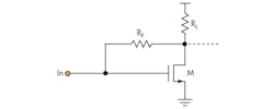
Figure 1 shows the basic topology of an amplifier with resistive-feedback input stage. The design can be studied with the simplified model depicted in Fig. 2. In addition, gain (A), noise figure (NF), and input impedance (Zin can be calculated using Eqs. 1, 2, and 3, respectively9:
|AV| ≈ gm x (RF x RL) (1)
NF ≈ 1 + [(2/(3gmRS)] x [(1/RS) + RS/ RF2] + [(2f2gmRS/3f2Tmin + (RS/RF) (2)
Zin ≈ (RF + RL)/(1 + |AV|) (3)
where:
gm = the transconductance of transistor M;
RL = the load resistance; and
RF = the feedback resistance.
The circuit is assumed to be connected to a source generator with source impedance, RS, that is typically 50 Ω.
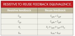
Resistive feedback can be implemented with a current-reuse technique, as depicted in Fig. 3(a).10 Stacking both NMOS and PMOS transistors, the overall equivalent transconductance is increased from gm to gmN + gmP for the same bias current. Furthermore, removing load resistance RL enables this configuration to maintain the transistors in the saturation region with a minimal supply voltage, and without design tradeoffs.6,9 In the current reuse configuration of Fig. 3(a), Eqs. (1) through (3) are kept the same according to the equivalent values listed in the table.
In the present amplifier design, an NMOS transistor replaces the traditional feedback resistor as shown in Fig. 3(b). In an ideal amplifier, the feedback resistance and gain characteristics are almost equivalent. The resistance value of the NMOS transistor can be derived as6:
rds ≈ L/[KW(Vgs - VT)] (4)
where:
K = Boltmann’s constant;
W = the effective channel width;
L = the effective channel length; and
VT = the threshold voltage.
Building Blocks
From Eq. 4, it can be seen that as VC changes, Vgs will change, then resistance rds will also change. Therefore, the feedback resistance is variable, as is the gain.
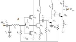
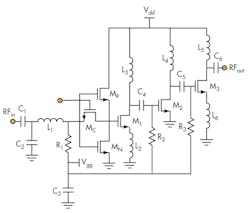
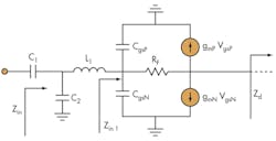
Figure 4 shows a complete schematic diagram of the 26-GHz CMOS VG-LNA. The preamplifier is comprised of a T-section matching network and a resistive-feedback current-reuse stage. Based on the methodology in ref. 10, simultaneously input impedance and noise matching at a frequency of 26 GHz was achieved by selecting appropriate values for the passive circuit elements C1, C2, and L1 and the size and bias of the input resistive-feedback current-reuse network. Figure 5 provides a small-signal equivalent circuit of the preamplifier. From Fig. 5, the input impedance of the small-signal equivalent circuit is given by11:
Zin = 1/sC1 || 1/sC2 + sL1 + Zin1 (5)
where:
Zin1 = 1/[Zd/( Zd + RF)] x [(gmN + gmP) + s(CgsN + CgsP)] (6)
and
Zd = the input impedance of the post-amplifier.
To achieve sufficient gain, the post-amplifier is comprised of three cascaded common-source stages and an output matching network. In the first stage, proper scaling of the transistor and gate inductance are used to shift optimum source impedance, Zopt, to 50 Ω, which makes it easier to achieve low noise figure. The output of each stage is loaded with a bandpass (or a highpass) combination of L and C to provide parallel resonance and to increase gain at the 26-GHz center frequency. Inductor L6, which is connected to the source of transistor M3, improves the stability of the LNA. The DC block, about 60 fF at the output, was chosen for output matching. Since this small capacitance might be sensitive to process variations, it has been composed of two MIM capacitors in series so as to desensitize the output matching from processing variation. The component parameters are as follows:
L1 = 414.8 pH;
L2 = 1 pH;
L3 = 327.4 pH;
L4 = 96.7 pH;
L5 = 260.7 pH;
L6 = 114.6 pH;
C1 = 7.6 pF;
C2 = 273.65 pF;
C3 = 4 pF;
C4 = 70 fF;
C5 = 10 pF;
C6 = 60 fF;
R1 = kΩ;
R2 = kΩ; and
R3 = kΩ.
The bias conditions are Vdd = +1 VDC and Vgg = +0.7 VDC. The CMOS transistors used in these circuits have been demonstrated to have cutoff frequency, ft, of around 50 GHz and maximum frequency of oscillation, fmax, of around 90 GHz. The excellent ft and fmax performance levels mean that it should be possible to use this CMOS process for high-performance K-band LNAs.
How It Stacks Up
Related Articles
• Broadband Radio’s LNA Shoulders Harmonic Rejection To 20 dB
• Balanced UHF LNA Simplifies Cell Towers
• Wideband LNA Spans 0.5 To 40.0 GHz
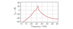
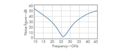
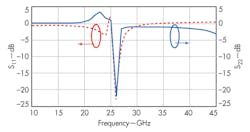
To demonstrate the effectiveness of the design approach, a 26-GHz VG-LNA was designed and fabricated using a standard 0.18-μm CMOS process from TSMC. The circuit draws only 6.48 mW from a +1-VDC supply. Results were obtained using the post-layout simulation features of the Advanced Design System simulation software from Agilent Technologies. Figures 6 and 7 show gain and noise figure, respectively, as functions of frequency. The small-signal gain has a peak value of 21.1 dB and the noise figure has a minimum value of 3.0 dB at 26 GHz. Figure 8 shows input and output return losses, with minimum input and output return-loss levels of 23.3 dB and 21.6 dB, respectively.
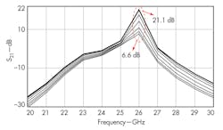
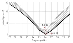
As Fig. 4 indicates, controlling the gate voltage VC for device MC in the first stage can provide controllable gain. As shown in Fig. 9, the VG-LNA achieves continuous gain adjustment range of nearly 14.5 dB from 6.6 to 21.1 dB when VC is varied from +0.6 to +1.0 VDC in 0.05-V steps. Figure 10 shows the noise figure for the VG-LNA when sweeping VC: the noise figure is varied from 6.5 to 3.0 dB when VC is varied from +0.6 to +1.0 VDC in 0.05-V steps.
In short, a VG-LNA for K-band applications has been presented. The designed VG-LNA is composed of a resistance feedback current reuse stage and three cascaded common-source stages, and is simulated based on TSMC’s 0.18-μm silicon CMOS process. By using a highpass combination of L and C circuit elements loaded on the output of each stage to provide parallel resonance, the VG-LNA consumes only 6.48 mW from a +1-VDC supply while attaining gain of 21.1 dB and minimum noise figure of 3 dB at 26 GHz. With a controlling voltage, the gain and noise figure can adjusted over reasonably wide ranges.
References
1. Y.-K. Hsieh, J.-L. Kuo, H. Wang, et al., “A 60 GHz Broadband Low-Noise Amplifier With Variable-Gain Control in 65 nm CMOS,” IEEE Microwave and Wireless Components Letters, Vol. 21, No. 11, 2011, pp. 610-612.
2. W.-C. Wang, Z.-D. Huang, G. Carchon, et al., “A 1 V 23 GHz Low-Noise Amplifier in 45 nm Planar Bulk-CMOS Technology With High- Q Above-IC Inductors,” IEEE Microwave and Wireless Components Letters, Vol. 19, No. 5, 2009, pp. 326-328.
3. S.-C. Shin, M.-D. Tsai, R.-C. Liu, et al. “A 24-GHz 3.9-dB NF low-noise amplifier using 0.18 μm CMOS technology,” IEEE Microwave and Wireless Components Letters, Vol. 15, No. 7, 2005, pp. 448-450.
4. S.-H. Yen and Y.-S. Lin, “Ka-band low noise amplifier using standard 0.18 μm CMOS technology,” Electronics Letters, Vol. 42, No. 16, 2006, pp. 919-920.
5. F. Yu and C. Wang, “CMOS LNA Boosts 64 GHz,” Microwaves & RF, Vol. 50, No. 10, 2011, pp. 64-77.
6. C. Wang, J. Jin, and F. Yu, “A CMOS 2-11 GHz Continuous Variable Gain UWB LNA,” IETE Journal of Research, Vol. 56, No. 6, 2010, pp. 367-372.
7. Y. Kim and Y. Kwon, “A 60 GHz Cascode Variable-Gain Low-Noise Amplifier With Phase Compensation in a 0.13 μm CMOS Technology,” IEEE Microwave and Wireless Components Letters, Vol. 22, No. 7, 2012, pp. 372-374.
8. C. Wang, J. Jin, and F. Yu, “Low-Power TIA Tunes Gain At 2.4 GHz,” Microwaves & RF, Vol. 49, No. 5, 2010, pp. 78-86.
9. T. Taris, J.-B. Begueret, and Y. Deval, “A low voltage current reuse LNA in a 130-nm CMOS technology for UWB applications,” in Proceedings of the 37th European Microwave Conference, Munich, Germany, 2007, pp. 1105-1108.
10. C.-W. Kim, M.-S. Jung, and S.-G. Lee, “Ultra-wideband CMOS low noise amplifier,” Electronics Letters, Vol. 41, No. 7, 2005, pp. 384-385.
11. W. Luo, C. Wang, and S. Du, “Design of 2-12 GHz Ultra-wideband CMOS low noise amplifier (in Chinese),” Microelectronics, Vol. 49, No. 2, 2010, pp. 243-247.
