Download this article in .PDF format
More markets are incorporating RF technology into their operating systems for a cornucopia of reasons, which are often specific to the industry. As a result, RF engineers have many new applications in which they can ply their trade. The first step—no matter what the industry or application—is to select an RF technology. Ultimately, this comes down to finding a technology that meets the size, heat, cost, speed, power, efficiency, and advancement rate needed for the application. Among the RF semiconductors competing for these myriad applications are silicon-based, laterally diffused metal oxide semiconductor (LDMOS), gallium arsenide (GaAs), and gallium nitride (GaN). Because each technology has its advantages and limitations, it is up to a shrewd engineer to sift through the possibilities.
When looking for an RF device technology for an application, it is important to remember that there are many legacy technologies still operating. Examples range from electron tubes for high-frequency heating and radio amplification to silicon bipolar transistors for legacy military/aviation equipment. Such device technology might still be used because mainstream technology cannot fulfill the very specific operating conditions involved. These specifications could be extremely high power (in the 100s of kilowatts) or extreme ruggedness and survivability.
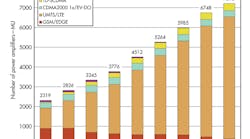
The military market, for example, is known for its use of legacy technologies. Yet the military/aviation-radar market—together with telecommunications—is growing quickly, driving the development of a lot of new microwave and RF technology. To get a feel for this growth and development, one can simply look to the power-amplifier (PA) market (Fig. 1). After all, RF PAs are used in most RF applications.
1. In a forecast by Strategy Analytics in January 2013, the market-research firm noted that the UMTS/LTE PA market is the fastest growing segment of PAs as LTE-A demands more complex capabilities.
Some mainstream device technologies, such as LDMOS and GaAs, have enjoyed consistent incremental growth and longevity in the RF markets. Both technologies have multi-decade histories of development and offer valued RF performance for a number of industries. LDMOS, for instance, is most commonly used for RF PAs for wireless infrastructure. These devices are constructed of an epitaxial silicon layer on a highly doped silicon substrate. LDMOS boasts high-output-power capability of tens to hundreds of watts, which corresponds to technology with 60-V drain-to-source breakdown voltage.
Generally, LDMOS devices operate below 3 GHz. However, companies like Freescale and NXP have announced that they are developing LDMOS technology that can operate efficiently to 3.5 GHz for wireless broadband applications. Because LDMOS is known for its rugged and reliable nature, it is often used in harsh environments like wireless base stations. When a technology has been in development for many years, the manufacturing costs also are conservative, making it attractive in that regard as well.
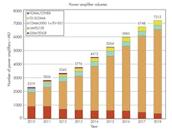
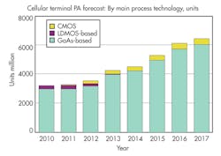
While LDMOS is a high-voltage, wide-bandgap semiconductor, GaAs operates at a lower power threshold of 10 to 12 V. GaAs is a wide-bandgap class III/V semiconductor with high saturated electron velocity and high electron mobility. As a result, GaAs transistors can potentially operate to 250 GHz. Because GaAs is highly resistive undoped, it provides isolation between microwave components. GaAs is commonly used for low-to-high-frequency and low-to-midrange-power applications, such as mobile handsets in the cellular market (Fig. 2). Generally, GaAs devices operate well below 50 W and benefit from small die size with high levels of amplifier efficiency.
2. International Business Strategies recently shared a forecast for power-amplifier volumes through 2018. It shows that UMTS/LTE technologies are leading the telecommunications technologyâs increase of PA production.
Where GaAs and LDMOS leave off in power and frequency capability, newer technologies like GaN are enabling new technologies.
GaN is a wide-bandgap semiconductor material that provides high levels of hardness, mechanical stability, heat capacity, and thermal conductivity. It also has very low sensitivity to ionizing radiation. This aspect opens doors for GaN to operate in satellite and military environments. The technology is well matched for high-power and high-frequency operation, which has encourage the exploration of is use into the millimeter-wave frequencies. In terms of power capability, GaN can reach hundreds of watts.
Generally, GaN technologies are placed on silicon-carbide (SiC) wafer substrates, as SiC beats GaN at distributing heat by almost a factor of three. According to Mike Mallinger, director of business development for Microsemi, “The problem with GaN is a thermal one. GaN-on-SiC leads to longer reliability.” Regarding the use of SiC as a primary technology, Mike commented, “Though SiC has a high breakdown voltage and thermal properties, its limited gain of less than 10 dB make GaN-on-SiC a more viable option.” This enhanced thermal process enables GaN-on-SiC for high-powered pulse applications, such as S-band radar for military and aviation. Although electron tubes traditionally dominated this market, GaN-on-SiC technologies enable much faster pulsing. In addition to those that it could displace, there are many applications that such a high-frequency and high-power device technology could enable.
GaN Vs. LDMOS
When asked about competition between LDMOS and GaN, Lance responded, “GaN is starting to capture some wireless-infrastructure sockets-- mostly for remote radio heads and active antennas. But silicon LDMOS still rules this space. It will be hard for GaN to really dislodge LDMOS for lower-frequency markets due to cost, but the GaN vendors are making progress in that regard GaN is still several times the price for die than LDMOS. As you go up in frequency, where the packaging and assembly become more costly than die costs, the cost difference starts to level out. For instance, an S-band-radar LDMOS device costs about the same as a S-band-radar GaN part.”A deluge of information is currently available about GaN’s performance and its potential in the marketplace. Some sources claim that it will overtake both the GaAs and LDMOS markets, among others. Lance Wilson, Research Director of RF Devices for ABI Research, sums up these considerations with the following: “Engineers need to look at device technology very clear eyed. There is a lot of hype right now about how GaN technology can do no wrong. GaN is not viable for every application and it can have cost issues. Above 3 GHz for high-power RF, though, GaN is generally a no-brainer.”
Of course, much hype has been devoted in recent years to whether GaN can replace GaAs in the bulk of its application. Lance summarizes, “Where the present application power line between GaN and GaAs lies is still a point of discussion. Some say 10 W and some say as much as 35 to 40 W, but 20 to 25 W seems to be a reasonable space.” His guess is that applications under 25 W or so are likely to remain GaAs.
The development of GaN on SiC devices is a main target for its potential to enable new high-power and high-frequency markets. This could include wireless backhaul, military/defense, satellites, and many more. The main drivers from these markets require this device technology to lower costs as the cost of SiC as a material and the small wafer sizes are limiting the cost conscious markets. Higher switching frequencies along with the inefficiencies caused by normally-on switches are other characteristics necessary for larger adoption of this technology.
Related Articles
• GaN-On-SiC Devices Power DC To 18 GHz
• Gallium Nitride Drives Power Amplifier Performance
• Beyond CMOS Vs. GaAs: Picking The Right Technology
As this technology naturally is very robust, reliable, radiation hard, and has a high breakdown voltage these are targeted characteristics for cost effective advancement. GaN and Si have significant thermal mismatch properties, which prevents easy integration. Development is being focused on enhancing the capability to incorporate GaN and Si for drop-in swap operation with Si. Increasing the availability of material sources and limiting defects in GaN technology are other aspects of the technology needing solutions. As GaN technology is invested in, many of these barriers are likely to fall to the wayside and will open doors for new RF possibilities.
Bright new technologies will always be driven forward with promises of enhancing existing RF industries and helping to create new ones. When considering device technologies, however, it is key that RF and microwave engineers look beneath the claims to find the option that is best for their application. Due diligence is required while weighing all of the specifications and parameters. As RF technology advances, it is likely that the present device technology will be supplanted by higher-performance, more cost-efficient or more reliable technologies. New device technologies shine in enabling advanced RF operation for fresh applications, which can best take advantage of these technologies’ unique benefits.


