Waveguide Diplexer Links Point-To-Point Systems
This file type includes high resolution graphics and schematics when applicable.
Point-to-point radios at 18 GHz link many different communications systems, including terrestrial and satellite-base systems. A key component for these systems is the diplexer, which helps to manage and sort multiple signals. Fortunately, a simple and efficient technique has been developed for designing a waveguide diplexer for 18-GHz point-to-point communications applications, and the design approach can also be extended to the design of general junction-type waveguide multiplexers.
Related Articles
• Millimeter-Wave Technology Prepares For A Wealth Of Applications
• LTE, WiFi, And WiGig Push Filter Capabilities
• Test High-Power RF/Microwave From Tower To Tabletop
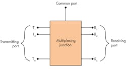
Microwave diplexers and multiplexers filter and separate the multiple frequency channels or bands in a common transmission line to direct each channel to its proper output port. In reverse, these components can combine signals of different frequencies at separate input channels into a single output port. Diplexers and multiplexers are essential when transmitting multiple, different-frequency signals through a single transmission medium, such as an antenna or transmission line.1Figure 1 shows a typical multiplexer. Signals for transmission (T1, T2, through Tm) are in the m channels, while the received signals (R1, R2, through Rn) are in the n channels.
In general, the channels in a multiplexer can be contiguous but not overlap. Typical microwave multiplexers are implemented in rectangular or circular waveguide,2 on printed-circuit boards (PCBs),3 and as ceramic structures.4,5 Bandpass filters with a narrow bandwidth and a sharp rolloff property are used in each channel to screen desired frequency components and reject unwanted out-out-band signals. Bandpass filters are combined at the multiplexing junction into the common port or vice versa.
The multiplexing junction is a crucial part of a microwave multiplexer. Major types of multiplexing junctions used in waveguide multiplexers include the circulator/filter chain, the directional coupler/filter scheme, the manifold structure, and the branching filter scheme.1 Mutiplexers employing the latter two structures are often called junction-type multiplexers. In junction-type multiplexers, impedance-matching elements are usually employed in the junction region to achieve low reflection at all bands. This article will focus on the design of junction-type diplexers.
Diplexers are multiplexers with two channels. They are used for separating or combining transmitted and received signals in single-antenna communications or radar systems. Using a simple approach, it is possible to design high-performance T-junction waveguide diplexers, and the basic idea behind the technique can be extended to the design of general junction-type multiplexers.
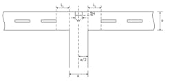
Figure 2 shows the structure of a diplexer designed with this simple approach. It consists of bandpass filters 2 and 3, operating at bands 2 and 3 respectively. The diplexer is implemented in rectangular waveguide with a broad wall width of a and a narrow wall height of b. In most standard rectangular waveguide structures, b is one-half the value of a. For this multiplexing junction, an H-plane T-junction with a septum matching element is employed. Other types of waveguide junctions and matching elements can be used as well.
Figure 3 shows the design parameters for the diplexer junction. A combination of a septum of suitable dimensions and distance L3 from the junction center line to the first element of filter 3 enables impedance matching at band 2. Similarly, for impedance matching at band 3, the distance L2 is optimized with proper septum dimensions. A common design approach is to represent the diplexer junction and channel filters with network parameters and to optimize the T-junction structure and distances from the T-junction to channel filters—and in some cases, the first few elements in the channel filters.6-10 The design of the diplexer junction can be greatly simplified with the aid of modern electromagnetic (EM) simulation software tools.
This file type includes high resolution graphics and schematics when applicable.
Getting Started
This file type includes high resolution graphics and schematics when applicable.
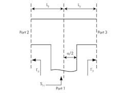
The first step in the diplexer design technique is to replace filters 2 and 3 with their respective reflection coefficients, Γ2 and Γ3, and to use the initial dimensions of the septum (as shown in Fig. 4, where the initial dimensions of the septum are set to zero). Values for reflection coefficients Γ2 and Γ3 are obtained beforehand by numerical simulation, using commercial simulation software such as Microwave Studio from Computer Simulation Technology, the High Frequency Structure Simulator (HFSS) electromagnetic (EM) software from Ansys, or even in-house EM computational programs. With this approach, one can avoid the mathematical manipulation of the admittance or scattering matrix of the T-junction.
The next step involves adjusting the distance L3 such that |S11| is at its smallest value at band 2. Since, by design, the filter 2 is well matched at band 2, distance L2 will have a negligible effect on |S11|. The distance L2 is determined in the same way for minimum value of |S11| at band 3. Lengths L2 and L3 should be large enough so that higher-order modes generated at the T-junction discontinuity and the septum are sufficiently attenuated after propagating over the distances L2 and L3. With the values for L2 and L3 determined, typical values for |S11| would be around -10 dB at each filter’s passband.
At this point in the design process, a septum with suitable height H and width W is added to reduce the value of |S11|. It has been found that |S11| is not sensitive to septum width W ranging from 0.05a to 0.30a. A septum width W equal to 0.30a is a good choice since it results in a mechanically stronger structure than when using a thin septum. With septum width W fixed at 0.30a, the septum height H can be adjusted until |S11| is at its smallest value for both bands. With a properly designed septum, |S11| is now decreased to less than -20 dB at both bands. If necessary, simultaneously adjustments can be made in L2, L3, and H for further improvements in |S11|.
This design technique can be extended to creating general junction-type multiplexers. In the first stage, each bandpass filter is replaced with its precomputed reflection coefficient, and the dimensions of the impedance-matching elements in the multiplexing junction are set to their initial values, which may all be zero. For impedance matching the multiplexer’s kth channel, the distances from all other filters to the junction reference plane are adjusted for the lowest reflection at the kth band. This process is then repeated for all channels. This completes one design cycle of the filter distance optimization. The filter distances will be changed in each step of a design cycle. Many cycles of the filter distance optimization is carried out until a convergence is obtained.
Next, the matching elements of the multiplexer junction are adjusted for good impedance matching at all bands. If desired performance is not obtained in the second stage, the first and second stages can be repeated or combined and simultaneously adjustments made to the filter distances and impedance-matching elements of the junction.
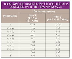
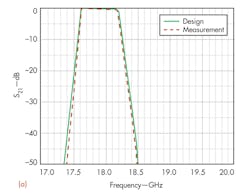
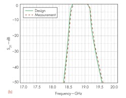
To demonstrate the effectiveness of this design approach, a waveguide diplexer was designed and fabricated. It is a diplexer fabricated with WR-51 waveguide, with a = 12.95 mm and b = 6.48 mm and with passbands of 17.7 to 18.1 GHz (band 2) and 18.7 to 19.1 GHz (band 3). Microwave Studio was employed in the numerical simulation. Waveguide filters of order 8 with thin metal strips along the waveguide center line were designed using the Rhodes method.11,12Figure 5 shows the structure of this experimental filter, with its dimensions shown in the table. The filter's order determines the rolloff rate.
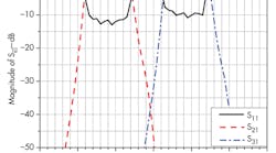
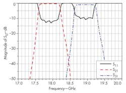
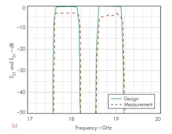
When two channel filters are combined in the H-plane T-junction without a septum and with filter distances L2 and L3 optimized, the resultant reflection coefficient shown in Figure 6 is only at a level of -10 dB. Using the septum in the T-junction, the reflection coefficient was reduced to a -20-dB level. The diplexer junction's final dimensions were L2 = 8.15 mm, L3 = 6.80 mm, W = 4.00 mm, and H = 2.10 mm.
This file type includes high resolution graphics and schematics when applicable.
Sizing Up The Diplexer
This file type includes high resolution graphics and schematics when applicable.
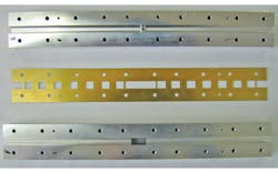
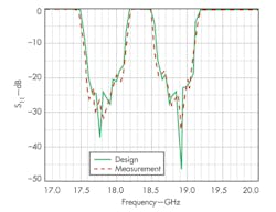
The experimental diplexer (Fig. 7) was fabricated using the split-block method.13 Its performance was evaluated by means of high-frequency measurements, with the measured results agreeing fairly closely with the simulations (Figs. 8 and 9). The diplexer exhibits a low passband insertion loss of 0.3 dB in band 2 and only 0.5 dB in band 3, compared to simulated insertion-loss values of 0.08 dB for both bands. The low insertion loss of the simulations is due in part because ideal conductors are assumed, with considerably lower insertion loss than actual conductors. As these results show, this approach helps to simplify the otherwise complicated design of a waveguide diplexer. When more channels are needed, it can also be applied to general junction-type waveguide multiplexers.
Acknowledgments
This work was supported by the National Research Foundation of Korea (KRF) grant funded by the Korean government (MSIP) (No. 2008-0062611).
Seong-Gon Choi, Professor
Department of Radio and Communications Engineering
Jargalsaikhan Nyambayar, Graduate Student
Eun-Jong Cha, Professor
Department of Medicine
Biering-Cheal Ahn, Professor
Department of Radio and Communications Engineering
Jae-Hoon Bang, Research Professor
BK21 Chungbuk Information Technology Center, e-mail: [email protected]
Chungbuk National University, 12 Gaesin-dong, Heungdeok-gu, Cheongju-si, Chungcheongbuk-do, South Korea; +82 43-261-2114
This file type includes high resolution graphics and schematics when applicable.
References
This file type includes high resolution graphics and schematics when applicable.
1. J. Uher, J. Bornemann, and U. Rosenberg, Waveguide Components for Antenna Feed Systems: Theory and CAD, Boston: Artech House, Norwood, MA, 1993.
2. J. Browne, “Waveguide diplexer extends to E-band,” Microwaves & RF, online, February 2012.
3. S. Caiou, C. Quendo, E. Rius, J.-F. Favennec, B. Potelon, R. Segalen, and F. Mahé, “An 11-18 GHz four-channel DBR multiplexer for electronic warfare systems,” Proceedings of the 39th European Microwave Conference, September 29 to October 1, 2009, pp. 679-682.
4. M.P. Busse, “White paper: ‘Disruptive’ ceramic technology enables spectrum management (part 1),” Microwaves & RF, online, October 2005.
5. M.P. Busse, “White paper: ‘Disruptive’ ceramic technology enables spectrum management (part 2),” Microwaves & RF, online, November 2005.
6. Y. Rong, H.-Y. Yao, K.A. Zaki, and T.G. Dolan, “Millimeter-wave Ka-band H-plane diplexers and multiplexers,” IEEE Transactions on Microwave Theory & Techniques, Vol. 47, No. 12, December 1999, pp. 2325-2330.
7. A. Morini and T. Rozzi, “Design of ‘optimum’ three port symmetrical junctions for diplexer application,” IEEE MTT-S International Microwave Symposium Digest, 1994, pp. 739-742.
8. X.-P. Liang, K.A. Zaki, and A.E. Atia, “A rigorous three plane mode-matching technique for characterizing waveguide T-junctions, and its application in multiplexer design,” IEEE Transactions on Microwave Theory & Techniques, Vol. 39, No. 2, December 1991, pp. 2138-2147.
Related Articles
• Millimeter-Wave Technology Prepares For A Wealth Of Applications
• LTE, WiFi, And WiGig Push Filter Capabilities
• Test High-Power RF/Microwave From Tower To Tabletop
9. K.-L. Wu and W. Meng, “A direct synthesis approach for microwave filters with a complex load and its application to direct diplexer design,” IEEE Transactions on Microwave Theory & Techniques, Vol. 55, No. 5, May 2007, pp. 1010-1017.
10. A.E. Atia, “Computer-aided design of a waveguide diplexer,” Proceedings of the IEEE G-MTT International Microwave Symposium, June 4-6, 1973, pp. 53-55.
11. J.D. Rhodes, “Design formulas for stepped impedance distributed and digital wave maximally flat and Chebyshev lowpass prototype filters,” IEEE Transactions on Circuits & Systems, Vol. CAS-22, November 1975, pp. 866-875.
12. Y.-C. Shin, “Design of waveguide E-plane filters with all metal inserts,” IEEE Transactions on Microwave Theory & Techniques, Vol. 32, No. 7, July 1984, pp. 695-704.
13. A.R. Kerr, “Elements for E-plane split-block waveguide circuits,” ALMA Memo 381, July 2001.
This file type includes high resolution graphics and schematics when applicable.
