Download this article in PDF format.
Gallium nitride (GaN) is quickly becoming the semiconductor material of choice for both RF/microwave and higher-wavelength devices. It has long been a semiconductor foundation for light-emitting diodes (LEDs) and has appeared as recently at the 2020 Consumer Electronics Show (CES) as the latest semiconductor technology for home battery chargers. The technology has perhaps its longest history in the RF/microwave industry in high-frequency semiconductor devices, where it serves as the active device replacement for traveling-wave tubes (TWTs) in high-power pulsed radar systems.
With a wide bandgap of 3.4 eV, GaN supports active devices with extremely fast switching speeds and high power levels. It features a large breakdown voltage, supporting highly efficient and compact pulsed amplifiers that achieve high output power levels in relatively small packages. In the simplest terms, GaN is capable of higher power density and efficiency in a smaller package than silicon (Si) or gallium-arsenide (GaAs) semiconductors.
GaN semiconductors have many advantages over legacy high-frequency, high-speed devices such as Si and GaAs. GaN is a binary compound that’s formed when one atom of gallium combines with one atom of nitrogen. The resulting material handles higher breakdown voltages and power levels than Si or GaAs, with fewer variations as a result of changes in temperature. In some applications, it can reduce manufacturing costs.
GaN is available to the RF/microwave industry in a wide range of products, from die-level wafers (Fig. 1) to rugged high-power packaged microwave amplifiers and transistors (Fig. 2). Increased interest in GaN as a starting point for optical diodes, including anti-bacterial ultraviolet (UV) lights in healthcare applications, expands potential applications for GaN transistors and semiconductor devices in automotive, consumer electronics, defense and aerospace, healthcare, and industrial power systems. GaN transistors serve as the active devices in systems ranging from wireless communications base stations to high-power pulsed military radar.
GaN substrates are not available as a naturally occurring compound. Like GaAs, it’s a semiconductor material formed in the laboratory, with properties that make it attractive for use as an electrical semiconductor substrate material. GaN substrates can conduct extremely large voltages relative to their mass, with minimal variations in electrical conductivity as a function of changes in temperature.
The thermal densities of GaN transistors are much higher than those of other semiconductor materials and device types. By creating an effective heat-flow path, such as through the base of a metal-ceramic package, a GaN high electron-mobility transistor (HEMT) can also be relied upon to generate and dissipate large amounts of power as heat. As a result, the device has become attractive to military users to generate the high-power pulsed signals of radar systems, on the ground and in the skies.
Among the problems in generating large power (and the associated heat due to losses) from a small package is the thermal dissipation and need to minimize the effects of heat on circuit performance. In addition to the transistor, the rising temperatures can also impact the performance of the circuit and its surrounding components mounted on the circuits. For that reason, many GaN devices are mounted on silicon (Si), silicon-carbide (SiC), or even silicon-germanium (SiGe) substrates to help draw heat away from the active device regions.
GaN-on-SiC and GaN-on-Si
As an example, Qorvo, once known as the starting point for many GaAs projects, now also offers GaN-on-SiC foundry services. The firm has served a wide range of customers, from cable-television (CATV) providers to the Defense Advanced Research Projects Administration (DARPA).
Qorvo’s model TGA2222, a monolithic GaN amplifier on a chip that provides 10 W output power from 32 to 38 GHz, shows how the company applies the technology to serve an expected need for 5G cellular base stations. It can be used in both pulsed and CW operation, and delivers at least 25-dB small-signal gain over that frequency range when operating at 640-mA quiescent current and 24-V pulsed voltage or 24-V CW voltage. It provides +40-dBm saturated output power over that frequency range. As an indicator of how it will be used at millimeter-wave frequencies, it’s well-suited for higher-frequency 5G base stations as well as in military radar systems.
To show the capabilities of its 0.15-μm GaN-on-SiC process, Qorvo recently developed the QPM1021 high-power amplifier device for use at lower frequencies. It’s designed for 10 to 12 GHz and can produce 100 W output power with 20-dB large-signal gain and better than 32% power-added efficiency. The device comes in a bolt-down ceramic package to dissipate heat. It’s matched at input and output ports to 50 Ω for ease of designing surrounding circuitry.
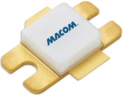
Long-time semiconductor supplier MACOM offers packaged GaN-on-Si power transistors rather than Si laterally diffused metal-oxide-semiconductor (LDMOS) transistors or GaN-on-SiC transistors. One example of the performance levels available from a GaN-on-Si RF transistor is the model MAPR-001011-850S00. The pulsed power transistor targeting avionics applications maintains rated output power of 850-W pulsed power from 1025 to 1150 MHz (10-μs pulse and 1% duty cycle).
MACOM also supplies the MAGB-107527-270-A0P, a 50-V, 50-W-output GaN monolithic amplifier optimized for wireless cellular base stations and digital predistorted modular signals from 2.5 to 2.7 GHz. It provides better than 12 dB of gain and 44% power-added-efficiency across the full frequency range. Despite its high-power level, the depletion-mode device comes in a compact plastic package.
Microchip Technology (formerly Microsemi) is another company with GaN-on-SiC RF power semiconductors in its arsenal. The devices feature S- and L-band pulsed radar amplifier output stages capable of generating large amounts of power from small packages. For example, model 2729GN-500V is an internally matched GaN-on-SiC packaged transistor well-suited for S-band pulsed radar systems. It’s capable of 500 W pulsed output power at 100% pulse width and 10% duty cycle from 2.7 to 2.9 GHz with more than 11 dB gain. The transistor and package are hermetically sealed for protection from the environment.
Wolfspeed, a Cree Co., has been an early supporter of GaN-on-SiC semiconductor technology and is a SiC wafer supplier (Fig. 3) to major semiconductor suppliers, including STMicroelectronics. Wolfspeed also markets its own GaN-on-SiC devices, such as the model GTRA384802FC. It’s a GaN-on-SiC HEMT in a ceramic package for cellular communications applications.
The single device delivers peak output power of 400 W and 63 W typical average power from 3.6 to 3.8 GHz while working from a +48-V dc supply. It achieves 42% efficiency with 13-dB power gain over the frequency range. With input and output ports matched to 50 Ω, the semiconductor device greatly simplifies the design of amplifier circuitry for multiple-standard cellular base stations.
The model GS66516B is among a number of enhancement-mode GaN-on-Si transistor dice and packaged devices available from GaN Systems. It’s supplied in a rugged and compact metal-ceramic package that’s based on the company’s patented Island Technology cellular layout to achieve high current capabilities with low inductance and low thermal resistance. The device is rated for 60 A and 600 V from drain to source and features a low drain-source capacitance. It’s a good fit for battery chargers, power supplies, and power converters. With low junction-to-case thermal resistance, it can dissipate the excess heat generated by high-power applications.
API Technologies supplies high-power GaN amplifiers for applications in defense electronic systems. The company details the progress that GaN solid-state devices have made in recent years with a white paper, “A GaN Solid-State Amplifier Replacement for a 1-kW Traveling Wave Tube.” The paper shows how API’s model QBS-609 GaN amplifier can replace a TWT, once considered the single point of possible failure in an airborne radar system. The amplifier measures just under 12 inches in length and is a footprint-fitting replacement for a commercial TWT amplifier, with several amplifier stages in a compact metal housing.
Taking integration somewhat further, NXP prepared for 5G wireless communications by launching its multiple-chip power modules with integrated Doherty amplifier and input and output ports matched to 50 Ω. The monolithic multiple-input, multiple-output (MIMO) module, with Si LDMOS power modules plus GaN-on-SiGe predriver modules and receiver modules, operates from 2.3 to 3.8 GHz with output power of 3 to 5 W. The company also supplies active power devices for aerospace and defense as well as for RF energy applications. For example, model AF1C31025GN is an RF GaN power amplifier mounted on a plastic flange-mount package. The device delivers 25 W of pulsed power from 2.4 to 3.1 GHz while operating on +32 V dc.
For those seeking a head start on GaN-based amplifier design, model IGNP3135M500 is an S-band radar amplifier module based on the GaN-on-SiC power semiconductor technology from Integra Technologies. It contains most of the amplifier circuitry preassembled and supplied in a compact modular-component package. The amplifier, a base-plate-cooled, pulsed RF GaN device, is designed to provide 500-W pulsed output power across a 400-MHz instantaneous bandwidth from 3.1 to 3.5 GHz. It operates at +50 V dc, achieves 50% efficiency, and can be supplied with input and output connectors as well as optional internal circuitry to monitor temperature and operating power levels (input, output, and reflected power).
If it’s transistor building blocks you’re looking for, the company stocks GaN-on-SiC power devices as well as legacy Si LDMOS devices. For example, for higher-frequency C-band radar systems, Integra Technologies has packaged power GaN-on-SiC transistors such as the model IGT5259CW25, which is matched to 50 Ω at input and output ports. It’s capable of 25-W CW output power from 5.2 to 5.9 GHz with 12-dB typical gain and 45% power-added efficiency when operating from a +36-V dc supply.
More GaN Options
With respect to its development efforts on GaN devices, Analog Devices expects to eventually reach beyond 50 GHz in producing gain and solid-state output power. The company plans to support semiconductor devices well into the millimeter-wave frequency range for such applications as 5G base stations and automotive safety systems, although its devices are presently reaching much lower upper-frequency ranges.
As an example, the model HMC1087 die is a GaN chip transistor MMIC power amplifier that can produce +39 dBm saturated output power with 11-dB small-signal gain from 2 to 20 GHz. The device input and output ports are matched to 50 Ω for ease of corresponding amplifier circuit design. The MMIC amplifier is a good fit for radar and communications systems in its frequency range.
To strengthen its position in GaN semiconductor technology, Swiss-based STMicroelectronics recently divulged its plans to acquire a majority stake in the French GaN epitaxial specialist Exagan. Of the acquisition, Jean-Marc Chery, the company’s president and CEO said, “ST has built strong momentum in silicon carbide and is now expanding in another very promising compound material, gallium nitride, to drive adoption of the power products based on GaN by customers across the automotive, industrial and consumer markets.
“The acquisition of a majority stake in Exagan is another step forward in strengthening our global technology leadership in power semiconductors and our long-term GaN roadmap, ecosystem and business,” added Chery. “It comes in addition to ongoing developments with CEA-Leti in Tours, France, and the recently announced collaboration with TSMC.”
STMicroelectronics already has a well-developed GaN semiconductor fabrication process in which a two-degree, high-electron-mobility gas layer is formed between an aluminum-gallium-nitride (AlGaN) buffer layer and the GaN substrate. The company serves a variety of markets, including power and safety, with products such as millimeter-wave (mmWave) automotive radar transceivers for advanced driver-assistance system (ADAS) applications at 24 and 76 GHz.
These monolithic chirp radar ICs, which come in miniature multilead plastic packages, can be used as the foundations for complete automotive radar safety systems. As an example, the company’s model STRADA770M is a radar transceiver in a transistor package with integrated frequency-modulated continuous-wave (FMCW) chirp modulator and a profiles-based sequencer for use in the 76- to 77-GHz and 77- to 81-GHz bands. Depending on the voltages supplied to it, the device can generate additional voltages as needed using integrated low-dropout (LDO) regulators.
This, of course, is just a sampling of commercial GaN devices currently on the market. With the automotive market quickly adopting ADAS radar systems and 5G requiring more bandwidth than currently available, semiconductor suppliers are being asked to make these active devices affordable at mmWave frequencies, and GaN is currently the semiconductor material of choice at those higher frequencies.
Rolling Your Own GaN Devices
For those who know what kind of GaN device they want to make, several foundries are available to fashion custom ICs and discrete devices. For example, Raytheon Co. is a Category 1A Trusted Foundry for the U.S. Defense Department for both GaN and GaAs.
The foundry fabricates GaN high-electron-mobility transistors, pseudomorphic GaN (pGaN), and metamorphic GaN (nGaN) devices. Raytheon’s Andover, Mass. facility also provides all of the services associated with a semiconductor foundry, including circuit design, layout, modeling, fabrication, test, and module design for the fabricated ICs.
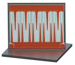
BAE Systems, another DoD-accredited partner, also provides GaN and GaAs foundries for industry use, backed by 6-in.wafer production runs. The foundry provides GaN-HEMT-based foundry services (see figure below) to the U.S. Department of Defense (DoD) and the design community at large for monolithic microwave integrated circuits (MMICs) from 1 to over 200 GHz. For those who prefer a variation, the foundry services from Wolfspeed are based on 100-mm-diameter, GaN-on-SiC IC technology backed by design and testing capabilities.


